
Ruben Ghulghazaryan, Jinhee Kim and Jeff Wilson, Mentor, a Siemens Business, Wilsonville, OR
Chemical-mechanical polishing (CMP) is an essential process in sub-micron integrated circuit (IC) manufacturing. Various ingredients are used to form a liquid slurry, which is then used with polishing pads to smooth (planarize) the surface of the wafer and remove deposits of specific materials. CMP is used when creating metal gates, front-end-of-line (FEOL) layers like shallow trench isolation (STI), and back-end-of-line (BEOL) metal layers, among others.
The success of the CMP process is strongly dependent on the design layout—in particular, on pattern density and other key geometric characteristics. Over- and under-polishing of patterns, dishing of wide trenches, and oxide erosion can all create problems during manufacturing, including difficulty meeting depth-of-focus requirements for lithography, multi-layer stacking effects creating shorts between nearby trenches, etc. To head off these negative impacts, foundry engineers typically perform modeling and simulation of the post-CMP surface profile during a topology and thickness prediction of a design, before any manufacturing begins.
However, in terms of time, wafers, and cost, the prediction of planarization failures or hotspots is actually far more effective when it is done during the design process, before the design is sent to the foundry. Because many CMP hotspots are due to design-specific layout issues, they can often be corrected with dummy fill, slotting, or the redesign of cells [1, 2]. Predicted topology changes due to erosion and dishing can be avoided with design adjustments that minimize these issues. Device damage that would occur during the CMP process can be minimized by fixing planarity hotspots before manufacturing.
Design-technology co-optimization (DTCO) is a collaborative methodology that encourages foundries, design companies, and electronic design automation (EDA) companies to work together to identify where and how manufacturing issues are created, then develop solutions to reduce or eliminate these issues at the most effective and efficient point in the design and manufacturing flow. For example, as part of a DTCO flow, foundries can use CMP model building and simulation to accurately predict hotspots and damage caused by the CMP process, then provide this information to the design team for use in design optimizations that enable the design to resist erosion and dishing defects during manufacturing.
DTCO Flow
SK Hynix and Mentor, a Siemens business, teamed up to create a DTCO flow built on CMP modeling and simulation, and analyze whether or not it can help avoid device damage during the CMP process.
CMP process effects
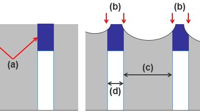
Figure 1 shows how some devices can be damaged by the CMP process. This specific type of device must have a rectangular vertical shape with well-defined right angles for proper functionality. However, it is very hard to control right-angle corners during several manufacturing processes. In particular, with respect to the designed device width and space characteristics, it is crucial to know how much the edge corners will be damaged due to dishing created during the CMP process.

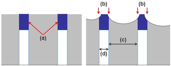
Figure 2 shows a simplified device formation process. The devices are formed by multiple deposition and etch processes on the substrate. Dielectrics fill the space between devices, and several deposited layers are used for more subtle control of the final CMP stop condition. The CMP process under consideration must be carefully controlled and stopped just on the top of polysilicon devices. In this example, however, the final CMP process damages the devices’ edge corners.

DTCO CMP modeling flow
By creating a highly accurate CMP model on a testchip, using measurements from specially designed CMP test patterns, foundries can determine predicted erosion and dishing. Design teams can use the results from these CMP simulations to predict device damage caused by CMP, and then implement layout optimizations to prevent or minimize this damage. To demonstrate this process, we created a CMP-impacted edge damage model.
In our use case, the process under consideration is oxide CMP, which should be stopped just on top of a poly hard mask layer. Poly lines must preserve their rectangle shapes in a cross-section view, but with the current layout, the edges are inevitably damaged by CMP dishing.
Testchip metrology and calibration
First, we designed a CMP testchip with specific test patterns for use in the CMP model building. A CMP model building test mask typically requires about 30-50 test patterns, with various combinations of line widths and spaces covering the possible structures of the real design.
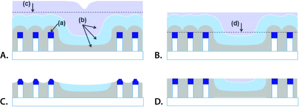
Next, we built a CMP model and calibrated it against our test data. CMP model calibration requires surface topology and thickness measurements both before and after the CMP process. We measured profile scan data after CMP for all blocks to get erosion and dishing measurements. We then used this measured erosion and dishing data, along with thickness measurements from cross-section images, for CMP model calibration (Figure 3).

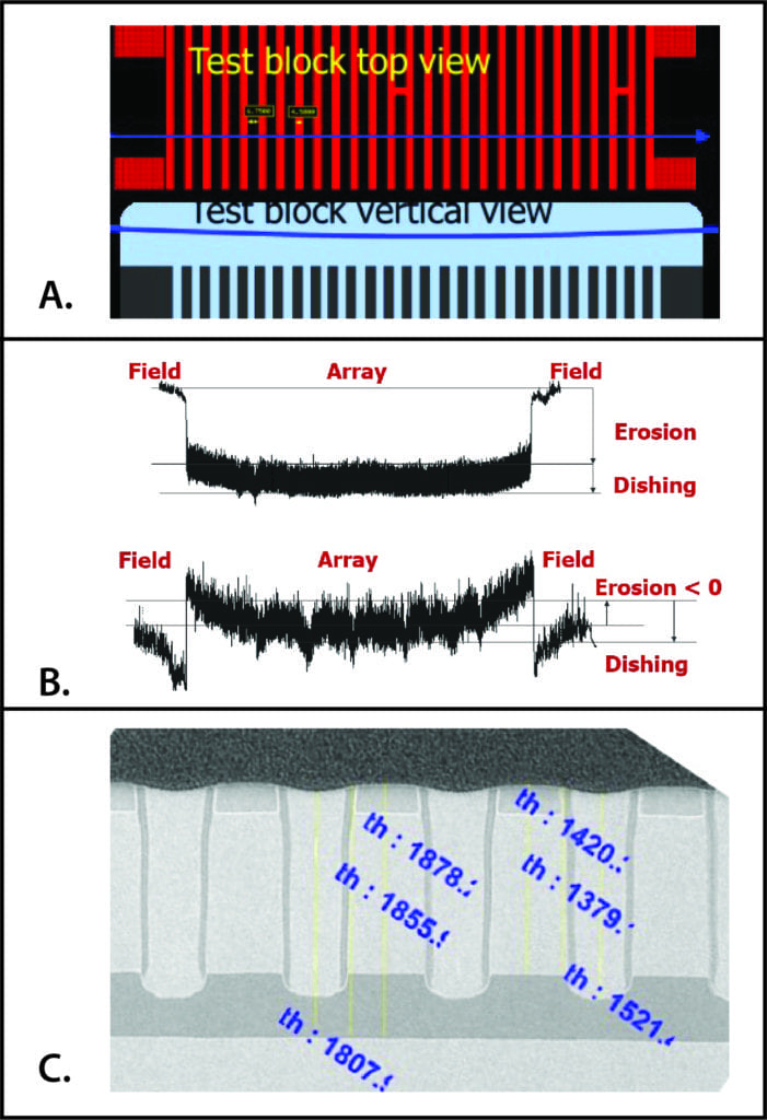
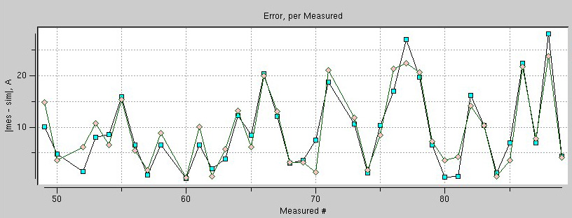
In our test case, we defined CMP dishing as device edge damage. The dishing measurements were collected by measuring edge damage using cross-section images, instead of profile scan data. The CMP model was calibrated with a less than 30A error in dishing prediction for all test blocks (Figure 4).

Once the model is calibrated, we can perform CMP simulations on production design layouts. Performing CMP simulation using our calibrated CMP model, we were able to predict, before actual mask tapeout and production, dishing hotspots on production designs that would likely result in device damage due to CMP.
Design optimization
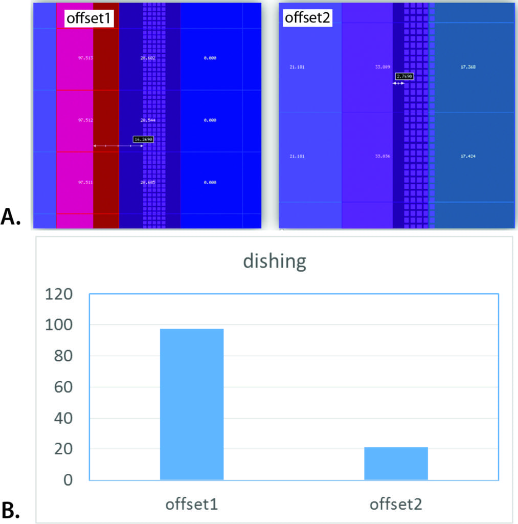
Based on these dishing simulation results, we were able to evaluate the design layout, and optimize the dummy pattern offset from the main patterns to avoid the predicted device damage (Figure 5). The number of dummy patterns used did not display any critical difference, so we were also able to minimize the use of dummy patterns to reduce the chip size.

In a real-world DTCO flow, manufacturing engineers create the calibrated CMP models and perform the CMP modeling and simulation on designs received for production. If hotspots are found, the designs can be returned to the design team with suggested design optimizations to eliminate or mitigate the predicted post-CMP issues. The use of CMP modeling and prediction as part of a DTCO flow can save both design companies and foundries the time and cost of manufacturing failures, improving yield ramp and accelerating market delivery schedules.
Conclusion
CMP damage can negatively affect design yield. Predicting CMP damage has always been a part of the manufacturing process, but in a DTCO flow, foundries can use CMP model building and simulation to inform design teams of predicted device damage due to the CMP process. Design teams can use this information to enable their designs to resist erosion and dishing defects before sending them to the foundry for manufacturing.
In our use case, CMP modeling was successfully used to predict device damage by simulating dishing and thickness variation induced by the CMP process. We then used this information to optimize the design to mitigate the actual dishing and thickness variation. By incorporating this kind of analysis and information exchange into a DTCO flow, foundries can help design teams modify their layout during the design flow, enabling them to deliver designs that are already protected against CMP defects. CMP modeling and process simulation are examples of critical elements that can be incorporated into a productive DTCO flow that enables both design companies and foundries to maximize market success.
Acknowledgments
The authors wish to thank YoungJu Lee, Jonghan Shin, and Eungrim Hwang of SK Hynix for their invaluable collaboration and contributions to this project.
References
1. U. Katakamsetty, D. Koli, Y. Sky, H. Colin, R. Ghulghazaryan, B. Aytuna and J. Wilson, “20nm CMP Model Calibration with Optimized Metrology data and CMP Model Application,” Proc. of SPIE, vol. 9427, 2015.
2. R. Ghulghazaryan, J. Wilson and A. Abouzeid, “FEOL CMP Modeling: Progress and Challenges,” Proc. of ICPT, pp. 34-37, 2015.