By Stephen M. Rothrock, President & CEO, ATREG, Inc.
The U.S. semiconductor industry is currently at a pivotal crossroads. In February 2024, U.S. Secretary of Commerce Gina Raimondo declared that CHIPS and Science Act investments will put the U.S. on track to manufacture roughly 20% of leading-edge logic chips used in advanced and emerging technologies such as artificial intelligence, quantum computing, and machine learning by the end of the decade. Today, U.S. fabricators make none of these chips. With the CHIPS Act funding nearly fully allocated, the new U.S. administration is now taking a hard look at the distribution of these funds, putting the validity of the CHIPS Act itself in question, and shifting the focus to understanding where the money went, leaving semiconductor companies uncertain as to what deals will go ahead and which ones may be altered. As the global semiconductor market lags behind more than anticipated and struggles to keep pace with rapidly evolving technologies, one question arises – who will shoulder the hefty financial burden required for the development of the next generation of semiconductor R&D and leading-edge innovation? This article delves into the complexities of these questions, exploring the current funding landscape, the challenges of advancing semiconductor technology, and the potential pathways forward for U.S. chip makers.
CHIPS Act funding recap
The CHIPS & Science Act represents one of the most ambitious federal efforts in decades to bolster domestic semiconductor production in the U.S. According to data collected by the Semiconductor Industry Association (SIA), the allocation of public funding has been divided into three primary sectors – approximately 68% directed towards front-end production, 14% towards the back-end sector, and a modest 16% to R&D. It includes a substantial $13 billion investment over five years in chip research and development (R&D) programs between the Department of Commerce ($11 billion) and the Department of Defense ($2 billion). At first glance, this funding mix suggests a strong emphasis on expanding fabrication capabilities – building new facilities, scaling up production lines, and modernizing equipment. Although both front-end and back-end are vital to the production chain, it is the relatively small slice allocated to R&D that is causing growing concern. The 16% set aside is expected to spur innovation in next-generation materials and processing techniques, yet many industry experts worry that this proportion may not be sufficient to meet the long-term demands of a competitive global market and that it leaves a critical gap when it comes to the innovative research required to push the boundaries of semiconductor technology.

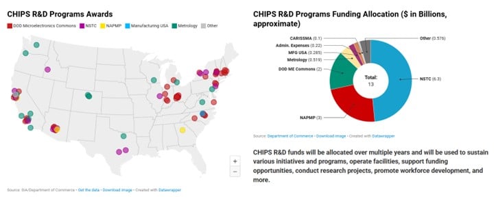
The cornerstone of the CHIPS R&D program is the National Semiconductor Technology Center (NSTC), a $5 billion public-private consortium established in February 2024 and tasked to “conduct research and prototyping of advanced semiconductor technology and grow the domestic semiconductor workforce to strengthen the economic competitiveness and security of the domestic supply chain.” Alongside it, the National Advanced Packaging Manufacturing Program (NAPMP) has awarded $1.4 billion in funding to bolster U.S. leadership in advanced packaging and enable new technologies to be validated and transitioned at scale to U.S. manufacturing. In October 2024, NY CREATES’ Albany NanoTech Complex was announced as the first CHIPS for America R&D flagship facility and planned site for the estimated $825 million CHIPS for America EUV Accelerator, another great example of industrial/academia collaboration expected to drive innovation in EUV technology and strengthen U.S. semiconductor leadership.
Challenges facing leading-edge R&D
Investing in leading-edge R&D is inherently risky and expensive, yet the race for capital expenditures (capex) is still raging among the world’s leading tech companies, reaching unprecedented levels in 2025, driven largely by the escalating demand for artificial intelligence infrastructure. Collectively, Meta, Amazon, Alphabet and Microsoft intend to spend as much as $320 billion on AI technologies and datacenter buildouts in 2025, based on comments from their CEOs early this year and throughout recent earnings calls. That’s up from $230 billion in total capital expenditures in 2024. Alphabet plans to invest approximately $75 billion in capex this year, focusing on technical infrastructure such as servers, data centers, and networking. Meta has announced its intention to spend between $60 billion and $65 billion to bolster its AI capabilities. Microsoft is committing around $80 billion towards AI-enabled data centers to support large language models and cloud-based applications.
The rapid pace of technological evolution means that semiconductor companies must constantly innovate to stay ahead of competitors, both domestic and international. However, with only 16% of CHIPS Act funding earmarked for R&D, many stakeholders question whether this is enough to sustain the breakthrough innovations necessary for the future. The nature of R&D in semiconductor technology requires not only significant financial investment, but also long-term commitment and collaboration between industry, academia, and government.
One of the biggest challenges is the high cost associated with developing new semiconductor technologies. As chips become more complex and the limits of traditional silicon-based manufacturing are tested, companies are forced to explore alternative materials and novel processes. Research in areas such as quantum computing, advanced photonics, and neuromorphic engineering demands a level of investment that may exceed the modest public funding available. Furthermore, the competitive global landscape, where countries such as Taiwan, South Korea, and China are ramping up their own investments, only intensifies the pressure on U.S. companies. Without adequate funding for high-risk, high-reward research initiatives, U.S. chip makers might find themselves outpaced by international competitors who are willing to invest more aggressively in the future of semiconductor technology.
Trump’s recent tariff announcements have introduced an additional layer of global economic and political uncertainty that could significantly impact funding for leading-edge R&D in the semiconductor industry. By driving up the costs of essential materials and with it overall fab construction, tariffs strain already tight capital budgets, forcing companies to reconsider or delay investment in long-term innovation. This uncertainty could create a “pausing effect” where chip makers adopt a wait-and-see approach, slowing progress in critical areas such as chip scaling, advanced lithography, and next-generation architectures – at a time when global competition in the sector is accelerating.
The role of GaN and SiC in next-generation chips
A key example of the challenges facing semiconductor R&D is the need to integrate emerging materials such as gallium nitride (GaN) and silicon carbide (SiC) into high-volume production. Both GaN and SiC are considered critical for applications requiring high power and efficiency – sectors that include artificial intelligence (AI), electric vehicles, renewable energy, and next-generation telecommunications. However, incorporating these materials into mainstream semiconductor production is far from straightforward.
GaN and SiC technologies traditionally operate at wafer sizes that are smaller than the industry standard 300mm format used in high-volume manufacturing. Transitioning these materials to 300mm wafer production is a formidable challenge, involving not only process re-engineering, but also significant capital investment in new equipment and retrofitting of existing fabs. The costs associated with scaling up these technologies could be astronomical, and with public R&D funding constituting only a fraction of overall CHIPS Act expenditures, semiconductor companies may have to turn to private financing or risk-sharing partnerships to bridge the gap. This situation poses an important question: if the current funding environment cannot support the necessary technological shifts, who will finance these critical upgrades?
“Chip makers have begun converting SiC devices to 200mm, but we have not seen any significant advances on the 300mm front,” explains Christian Dieseldorff, Senior Principal for Semiconductors of the Market Intelligence Team at SEMI. “However, GaN is a different story. Back in September of last year, Infineon succeeded in developing the world’s first 300mm power GaN wafer technology, the first company in the world to master this groundbreaking technology in an existing and scalable high-volume manufacturing environment. One month later, Texas Instruments announced that it has successfully developed GaN on 300mm wafers. This is exciting news!”
The integration of GaN and SiC into the production mix is not simply a matter of enlarging wafer sizes. It requires a comprehensive overhaul of processing techniques, quality control protocols, and supply chain logistics. Each of these factors adds another layer of complexity and cost, further stressing the importance of robust R&D investment. In this context, the current allocation of CHIPS Act funding might be seen as short-sighted, emphasizing production capacity at the expense of the innovation that drives the industry forward.
Retrofitting existing fabs to meet future demand
The first practical challenge U.S. chip makers face is the retrofitting of brownfield wafer fabs to accommodate next-generation manufacturing requirements. Many of these facilities were designed for traditional silicon-based chips and may not be easily adaptable to the new processes required for GaN, SiC, or other emerging technologies. Upgrading these facilities involves significant retooling and modernization, which can be both costly and time-consuming.
Retrofitting current fabs requires a careful balance between leveraging existing assets and investing in new capabilities. Semiconductor companies must assess whether the costs of modifying their current production lines can be justified by the potential gains in efficiency and technological advancement. This decision-making process is complicated further by the rapid pace of technological change, where today’s state-of-the-art equipment may quickly become obsolete. Additionally, the supply chain for advanced materials and components must evolve in tandem with these upgrades, creating additional logistical hurdles.
Public-private partnerships might offer one solution, providing a mechanism for sharing the risks and costs associated with retrofitting existing facilities. Collaborative efforts between government agencies, industry players, and academic institutions could lead to innovative approaches that make the transition smoother and more economically viable. However, establishing such partnerships requires clear strategic direction and long-term commitment – elements that are currently in flux as policymakers and industry leaders debate the best path forward for U.S. semiconductor manufacturing.
“Since our acquisition of the former TSI Roseville, CA fab in August 2023, we have begun the process of transforming the site to produce and test the first chips on 200mm wafers based on our pioneering SiC technology as soon as 2026,” explains Thorsten Scheer, Regional President of Bosch’s Automotive Electronics Division in North America and Plant Manager of Bosch’s Roseville, CA fab. Bosch has stated its intention to invest up to US$1.9 billion into the site.
Looking ahead: Financing the future of semiconductor innovation
The future of the U.S. semiconductor industry hinges on the ability to invest adequately in leading-edge R&D and to retrofit existing production facilities for emerging technologies. With global competitors such as China investing heavily in innovation and production capacity, U.S. chip makers must find creative ways to fund the transition to next-generation manufacturing. This may involve a combination of increased private sector investment, more substantial government support, and collaborative funding models that spread risk across multiple stakeholders.
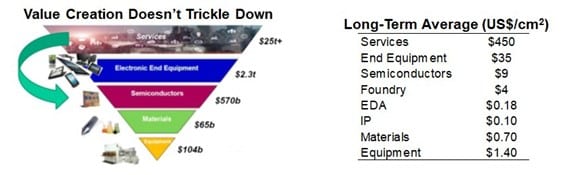
Value creation in the semiconductor industry often fails to trickle down due to its highly capital-intensive nature, where significant profits are concentrated among a few dominant players controlling critical parts of the supply chain, such as advanced chip design or fabrication. The industry’s steep barriers to entry, reliance on intellectual property, and regional monopolies in manufacturing or materials create imbalances in value distribution. Moreover, intense competition and rapid technological obsolescence pressure downstream firms, limiting their ability to capture or pass on value. As a result, smaller players and labor forces often see minimal benefit from overall industry growth.

“Government support for the chip industry is vital, but not the means to the end,” explains Malcolm Penn, Founder, Chairman, and CEO of British semiconductor industry research firm Future Horizons. “Government priorities change on an election cycle basis, whereas industry support is a continuum. The missing link? The end-user IDMs, especially the ‘Magnificent 7’and the mega-rich fabless firms, all of whom design state-of-the-art chips needing bleeding-edge technology but bootstrap a free ride on the cost of delivering this capacity. I think it is time for a new business model whereby semiconductor companies step up to the plate and share the financial responsibility of this effort.”
According to SEMI, semiconductor companies currently invest on average between 15% to 20% of their annual revenue in R&D. Tax incentives are a crucial tool for attracting U.S. semiconductor investment, with one key benefit – to strengthen innovation and drive technological advancements by allowing companies to reinvest savings into next-generation chip development. Increasing federal R&D tax incentives will allow semiconductor firms to invest more in AI chips, quantum computing, and advanced chip architectures. Additional funding for R&D and advanced packaging capabilities will ensure the U.S. maintains leadership in cutting-edge semiconductor technologies.
Ultimately, the question of who will pay for leading-edge semiconductor R&D remains unresolved. The CHIPS Act has laid the groundwork by injecting substantial public funds into the industry, but the allocation of these funds reveals a potential imbalance. If the current focus remains skewed towards immediate production capacity rather than long-term innovation, the U.S. risks falling behind in the global semiconductor race. Addressing this challenge will require not only increased investment in R&D, but also a strategic rethinking of how existing manufacturing infrastructure can be modernized to meet future demands.
About Stephen M. Rothrock


Stephen Rothrock founded ATREG in 2000 to help global advanced technology companies divest and acquire infrastructure-rich manufacturing assets, including wafer fabs (front- and back-end) as well as MEMS, solar, display, and R&D facilities. Over the last 25 years, his firm has completed 40% of all global operational wafer fab sales in the semiconductor industry, a total of 60 transactions. Recent global acquisitions and dispositions have involved ON Semiconductor, Allegro MicroSystems, Bosch, Elmos, Fujitsu, GLOBALFOUNDRIES, IBM, Infineon, Japan Display, Maxim, Micron, NXP, onsemi, Sony, Qualcomm, Renesas, Texas Instruments, and VIS to name just a few. Prior to founding ATREG, Stephen established Colliers International’s Global Corporate Services initiative and headed the company’s U.S. division based in Seattle, Wash.
Before that, he worked as Director for Savills International real estate brokerage in London UK, establishing their global corporate services platform serving large multinationals, many of whom were leading technology companies. Stephen also served on the UK-listed property company’s international board. He also spent four years near Paris, France working for an international NGO. Stephen holds an MA degree in Political Theology from the University of Hull, UK and a BA degree in Business Commerce from the University of Washington in Seattle, USA.