ZALA AJAYSINH, RAKESH GOSAI, SYAMALARAO GORUPUTI and DEVARAJAN DORESWAMY, eInfochips, an Arrow company.
In physical design, the goal is to achieve better Area, Power and Timing. To achieve this, we focus on place and route of design with equal importance given to the clock structure. According to the design requirement, we use different clock structures.
This paper will give an overall idea of some widely used clock structures with emphasis on practical implementation of conventional clock tree structure along with H-Tree. For the example provided here, the implementation was done on a real time database with operating frequency of 537MHz and 1.4 million instance count for 16nm technology node.
This paper also describes the types of cells and routing used for implementation of H-Tree clock structure, customization of H-Tree clock structure based on sink distribution, and various scenarios to be taken care of while choosing this approach. Comparison of clock-qor between this approach and conventional clock tree structure is given and it shows promising improvement.
Types of CTS clock structures
The main requirements for a clock tree structure are:
- Minimum Insertion Delay: A clock tree with minimum insertion delay will reduce clock tree power dissipation due to few clock tree buffers, uses less routing resources.
- Minimum skew: Minimum skew helps with hold timing closure. However, a tight skew requirement will lead to increase in clock insertion delay, which in turn leads to increase in the clock network power.
- More Common Paths: Having more common paths between launch and capture flop reduces the impact of OCV effects. The variations will cancel each other when the sinks share the same clock path to the root as any process-variation occurrence in that path affects both flops equally.
- Low Power Dissipation: A good clock tree structure should support implantation of clock gating to save the power.
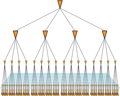
Conventional CTS (Figure 1) has been the default choice for most of the designs with lower frequency and less number of sinks, due to its ease of implementation.

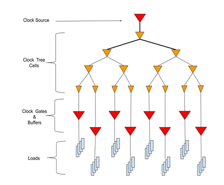
Conventional CTS may not be optimal choice for:
- Designs with high clock frequency
- Designs with high number of sinks
- Designs with sinks spread all over the core area
Advantages
- Simplicity of implementation
- Better clock gating, allows to do clocking at root level
- Low power consumption
Disadvantages
- Sensitive to on chip variations as sinks shares fewer common paths
- Higher insertion delays
- Difficult to achieve low skew due to asymmetric distribution of sinks
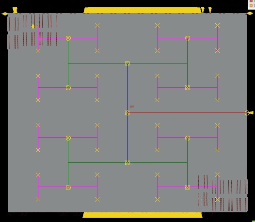
Mesh Structure
Clock mesh structure (Figure 2) produces lower clock skew and it is more tolerant to on-chip variations compared to conventional CTS.

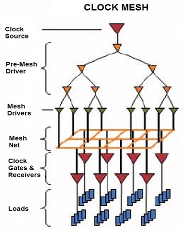
In the mesh structure, there will be a network of pre-mesh drivers to drive the clock signal from clock port to input of mesh drivers. The output of all the mesh drivers will be shorted using a metal mesh, which will carry the clock signal across the block using horizontal and vertical metal stripes. Clock to the sinks will be routed from its nearest tap point from the mesh.
Advantages
- Low clock skew
- Highly tolerant to the on-chip variations because of more common paths from the clock root to sink pin
- Possible to achieve lower insertion delays
Disadvantages
- High power (dynamic) consumption due to the parallel drivers driving the high capacitive load created by the mesh
- Requires more routing resources to create mesh
- Inability to use clock gating in different levels of the structure – the gating has to be performed at the local level only.
- Difficult to implement
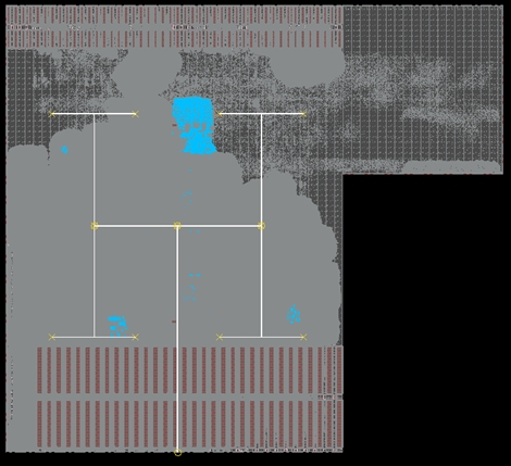
H-Tree
H-Tree structure is based on equalization of wire lengths. An ideal H-Tree (Figure 3) will see same length of wire segments and similar kind of drivers from its clock root pin to the output of last level drivers. The outputs of last level buffers will act as tap points and the sinks will have their clock routed from the nearest tap point. It provides good OCV tolerance because of more common paths.
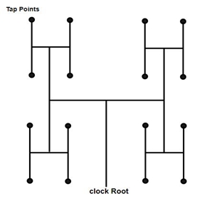
An ideal design for H-Tree is the one with no RAMs, ROMs, or other hard blocks. Design with blocks (macros) may create obstructions that prevent the placement of H-Tree super drivers from its ideal location. The lack of obstructions also enables the H-Tree routes to be perfectly straight, making it easier to ensure an ideal balance.
Advantages
- Possible to achieve low skew due to its symmetry
- Good OCV tolerance because of more common paths
- Less power dissipation compared to clock mesh
- Uses less routing sources compared to clock mesh
- Some high insertion delay compared to mesh. but lower than the conventional CTS
Disadvantages
- Difficult to implement and requires manual assistance to deal with blockages caused by macros and power connections
- Need drivers with high drive strength and these drivers should be surrounded by de-cap cells to avoid IR drop violations
- H-Tree wire segments should be routed with extra care to avoid signal integrity issues (EM)
Multisource CTS
Multisource CTS (Figure 4) is a hybrid approach and it offers the best of conventional clock tree and clock mesh. It has a coarser mesh structure compared to clock mesh, driven by mesh drivers. In general, there are three to nine levels of buffer or clock gating after mesh.

Advantages
- Higher amount of common paths than conventional clock tree which makes it more immune to OCV compared to conventional tree
- Less power consumption than clock mesh due to coarse mesh fabric
- Requires less routing resources compared to clock mesh
- High flexibility of implementation for macro dominated design in comparison to clock mesh
- Lesser skew in comparison with conventional clock tree
- Lesser insertion delay
- Ease of power gating
Building an H-Tree: A practical approach
H-Tree building is mainly divided into the following three major steps. It starts with the clock root pin defined, for which we want to create conventional clock tree structure and H-Tree.
Placement of Clock Tree: In this step, High drive strength ((X96/X128)) clock cells will be placed based on a given predefined location. These locations are mainly governed by the types of H-Tree customization needed to cater to block requirement.
Routing of Clock Tree Net: Routing of clock tree net is done keeping the below points in mind. They are also assigned specific NDR and given ‘don’t touch’ on these clock tree nets.
- All routes should be as straight as possible to minimize skew.
- All routes should be in the top metal layer.
CCOPT from Anchor Point: H-Tree endpoint will be treated as an anchor point. The tool will do CCOPT from the anchor point. We will set attribute to CCOPT; so, it will balance sink of all anchor points. CCOPT will also distribute and, if needed, swap sink among all anchor point to achieve the target latency and skew.
Data comparison: Conventional CTS vs Conventional CTS +H-Tree
The following table shows clock-qor comparison between conventional CTA and conventional CTS + H-Tree.
| Sr. No. | Parameter | Conventional CTS | Conventional CTS+ H-Tree |
| 1. | Max / Min Clock Level | 32/47 | 12/20 |
| 2. | Latency | 1.177ns | 0.449ns |
| 3. | Skew | 0.143ns | 0.110ns |
| 4. | Power | 1007mW | 994mW |
| 5. | Total Clock BUF/INV | 23000 | 21323 |
| 6. | CTS Routing Layer | M2 to M9 | M10 & M11 (H-Tree) M4-M9 (conventional CTS from the anchor point) |
| 7. | CTS Cell | P8U20A_CKINVX16 | P8U20A_CKINVX16 P8PU20A_CKINVX96 |
Table 1
Comparison done with below clock specification: Frequency: 537 MHz, Sink: 404896, Technology: 16nm, Instance: 1451840
Sample examples from actual projects using H-Tree
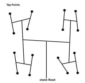
Figure 5a is the default H-Tree structure and Figure 5b and 5c shows its variations according to distribution of sink in the design.
Figures 5b and 5c show a case of H-Tree customization, wherein sinks are distributed locally. As highlighted, we need not to generate a default H-Tree structure and customized H-Tree structure (highlighted in red) suffices the block latency and skew requirement.
H-Tree Checklist
H-Tree overlap:This issue will be generally found in Macro dominated designs.
- Macro to super buffer overlap – To fix this we can refine the H-Tree cell location
- Multiple H-Tree super buffer overlap – Need to specify different offset to each H-Tree to avoid overlap between different H-Tree super buffer.
H-Tree Routing: Should be in top layer (M10-M11).
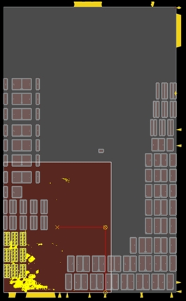
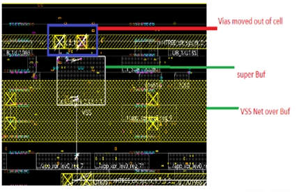
H-Tree Via: In order create robust H-Tree via structure, via stacks should be dropped on output pin of super buffer. Figure 6a shows that stack via was not dropped on output pin of super buffer because of VSS Net over super buffer.
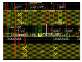
H-Tree stack via issue was resolved by refining cell placement of super buffer. As shown in Fig.6b, stack via dropped over super buffer output pin.
Future Scope
Rectilinear block: This clock structure works well in the rectangle block, however but will need modifications of structure for rectilinear block.
Multiple H-Tree: When we have multiple H-Tree, depending on the congestion and density of the block there could be H-Tree shorts in the CTS structure due to overlapping of the trees. We can further modify script to address this issue at the clock stage.
Conclusion
These H-Tree clock networks may be an alternative to the more traditional clock distribution networks.
The proposed clock tree optimization methodologies reduce the power dissipation without any impact on signal characteristics. The inductive behavior of the interconnects are reduced decreasing inductive noise.
In conclusion, when there is a tight skew requirement of 80~100ps and latency requirement <500ps and number of sink more than 10,000, using the H-Tree structure will be able to achieve better power, latency and skew.
Suggested additional reading
1. https://www.design-reuse.com/articles/21019/clock-mesh-benefits-analysis.html
3. https://www.electronicdesign.com/products/introduction-multisource-clock-tree-systems