
RYOUNG-HAN (RYAN) KIM, imec
Manufacturing chips for advanced logic applications starts with designing the electrical circuit. This process happens at different levels: from transistors over standard cells and place-and-route, up to the system design level. The patterns forming the circuit design layout are then written onto a photomask. Today, this is done by mask writing tools that make use of electron beams, such as the variable shaped beam (VSB) mask writer and multi-beam mask writer (MBMW). Next, in a photolithography exposure step, the pattern on the mask is downsized and projected onto the photoresist layer on top of the target wafer. After the resist development, the printed pattern is further transferred into the underlying layers of the substrate using advanced patterning and etch techniques.
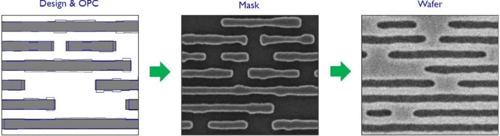
During the photolithography exposure step, the intended circuit layout image gets distorted. This is due to the way light propagates through the lithography scanner and mask, undergoing diffraction. The distortion translates into poor image fidelity, which is the difference between the target image and the printed structure on the wafer. The latter appears with irregularities such as line widths that are narrower or wider than designed, compromising edge placement integrity and resolution. Optical proximity correction (OPC) techniques are, therefore, applied to the layout design data: they correct the pattern before it is written on the mask to minimize errors from design to wafer.
Advancements in photolithography, mask, and OPC technology have been pivotal in driving the power-performance-area-cost (PPAC) improvements of subsequent logic technology generations. Resolution enhancements have been achieved by reducing the wavelength of the light used for the exposure step or by increasing the numerical aperture (NA) of the lithography scanner. Examples of the latter are the evolution from 193nm to 193nm immersion lithography, extreme ultraviolet lithography (EUV) and the forthcoming move to 0.55NA extreme ultraviolet lithography (High NA EUV).
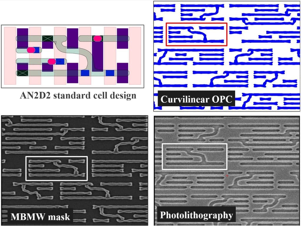
The design side also evolved to keep pace with the resolution enhancement offered by improved photolithography techniques. The pitch scaling demanded by successive technology nodes outpaced the advancements in photolithography. When that happened, designs for advanced logic chips moved away from 2-D Manhattan to 1-D Manhattan-based circuit layouts in the critical layers (FIGURE 1). In 2-D Manhattan-based designs, rectangular structures are used to align along both vertical and horizontal directions. In contrast, 1-D designs in the critical layers align structures to either vertical or horizontal directions per layer. Although 1-D Manhattan offers a dense representation, it comes with a downside: when making an electrical connection from one metal line to a neighboring one, an extra layer with a number of vias has to be implemented – adding to the wafer cost, and the path length of the electrical current.

In all this, there is one ‘peculiarity’: although designers today pursue rectangular, Manhattan-shaped structures in their design, the structures always appear as curved on both mask and wafer (FIGURE 2). This is an inherent consequence of how the mask writer and lithography scanner operate, acting as a low-pass filter for electron beams and light, respectively. Manhattan designs, therefore, become curved when transferred through the system, inducing additional errors in the final patterns.

Introducing ‘curvilinear’ in OPC and masks: reducing errors and improving the process window
A few years ago, the lithography community started exploring the idea of introducing curvilinear shapes when writing circuit patterns onto the photomask. This was facilitated by the emergence of the multi-e-beam mask writing tool, which, for the first time, enabled complicated shapes to be written on the mask. This assists in further minimizing the errors that occur along the path from Manhattan-based designs to curvilinear representations on the wafer.
More recently, the community also considered using new OPC algorithms that adjust the Manhattan design layouts towards the more complex curvilinear shapes on mask and wafer. Novel ‘curvilinear’ OPC techniques in conventional OPC and inverse lithography technology (ILT) started to emerge as a way to improve the process window of the photolithography step.
Both curvilinear mask and OPC techniques have recently become hot R&D topics in the semiconductor industry, which is reflected by the growing number of contributions at the 2025 SPIE Advanced Lithography and Patterning Conference.
Introducing curvilinear in the design space: node-to-node transitions at reduced wafer cost
Curvilinear OPC and mask strategies both still start from Manhattan circuit design layouts. As a next step, imec proposes to introduce curvilinear geometries and paths already in the design phase, an innovative concept with far greater benefits than curvilinear OPC and mask strategies. Opposed to current roadmap evolutions, curvilinear design promises to enable technology node transitions at reduced wafer manufacturing cost while improving electrical performance [1-2]. It is, therefore, believed to transform the semiconductor industry, as shown by imec in an invited paper at the 2025 SPIE Advanced Lithography and Patterning Conference [3]. The benefits are demonstrated with three use cases.
Click here to read the full article in Semiconductor Digest magazine.