By GOPAL RAGHAVAN, Ph.D., co-founder, Chief Technologist and SEMIR HADDAD, Senior Director Product Marketing, Eta Compute, Westlake Village, CA
These last years have seen a renewed interest in machine learning and artificial intelligence, thanks to the tremendous progress made at universities and publicized by internet giants and, the numerous use-cases found for neural networks in autonomous vehicles, surveillance cameras, healthcare, and e-commerce.
However, deep learning has not yet reached the very edge of the electronic world with devices operating on microcontrollers, with strong constraints on power consumption and limits on performance. A new technology, brought by Eta Compute, will change the game and make neural network inference at the extreme edge a reality.
The case for deep learning
Artificial intelligence covers many domains, from problem-solving and decision making to planning and natural language processing. In each of these domains, researchers and practitioners have developed a wealth of techniques that showed good enough results to be used in real-life examples and designed in commercial products.
Amongst these technologies, machine learning has received much attention lately, thanks to well-publicized achievements by leading deep learning teams. Deep learning algorithms have demonstrated par-human ability in various domains: image classification, game playing, lip-reading, speech recognition.
Besides their undeniable success, deep learning and artificial neural networks have several advantages versus other techniques that justify the excitement. Non-machine learning algorithms suppose a knowledge of the world that the human designer must translate in his algorithm. Traditional machine learning algorithms like decision trees and linear regression require an excellent understanding of the features that have an impact on learning. These two approaches thus require expert knowledge of the domain of study, leading to the fragmentation of artificial intelligence in many sub-domains.
Deep learning is different in that it does not require an excellent understanding of features and domains. Given a baseline understanding of significant inputs, it can extract features without designers having to analyze the data. Deep learning neural networks are, in fact, universal function approximators and given enough data, and they will approximate any function. This property was formally demonstrated in 2017 by Lu Et al [1].
Adding to this intrinsic benefit, the humongous amount of data made available with the internet, and the availability of common frameworks like TensorFlow and PyTorch, deep learning is quickly becoming a common language for all fields of artificial intelligence (AI). It is unifying the AI community, and most applications that used proprietary algorithms in the past have adopted at least some level of deep learning.
Deep learning at the extreme edge
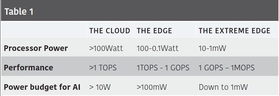
A continuum of devices: Deep learning algorithms first appeared in supercomputers and data servers for the enterprise, then on web and SaaS applications and later made their way into the internet of things: voice assistant, semi-autonomous cars, surveillance cameras, mobile phones. There is a continuum in power, performance, and cost between these products, and the next logical step is for neural networks to reach the extreme edge: the billions of devices that take care of most sensing and actuation in our daily life. Table 1 lists requirements for the cloud, the edge and the extreme edge.

The extreme edge devices are the ones that we see every day and don’t even think of as being intelligent. They are, however, the majority of the IoT devices:
- Building: thermostats, smoke detector, alarm sensors
- Home consumer: washing machines, remote control, TV, earbuds
- Medical and fitness: fitness band, health monitor, patches, Hearing aid
- Logistics: asset tracking, retail beacon, remote monitoring
- Factory: motors, industrial networks, industrial sensors
The data challenge and the rise of AIOT
It is now 20 years since the “Internet of Things” was first coined by Kevin Ashton, founder of MIT’s Auto-ID Lab in a presentation to Procter & Gamble. The IoT is becoming a reality, with billions of devices connected to the cloud.
The rise of the IoT comes with a challenge that was not wholly understood then: the management and cost of data. According to IDC, at the current rate, IoT Devices are expected to Generate 79.4ZB of data in 2025. All that data has an impact on the sustainability of the IoT and it’s ROI:
- Storage cost: data must be stored somewhere and maintained at a growing cost
- Security and Privacy: during its transfer and in the cloud, data is vulnerable to security and privacy breaches
- Communication cost: transferring data from the IoT device to the cloud has a price paid to the network operator
- Real-Time Response: Transferring data to the cloud increases latency and limits the real time capability of the IoT system.
Therefore, it is desirable to manage as much data as possible on the IoT device itself, where it is secure, and extract only the actionable information to be sent to the cloud. Several cloud companies and IoT industry leaders already championed the idea of moving more intelligence to the IoT device, also called the AIOT: Artificial Intelligence IoT.
The challenges of deep learning at the extreme edge
Like IoT before, AIOT holds great promise, and has its own set of challenges, due to the unique nature of the extreme edge.
The power constraint: Extreme edge devices have severe restrictions on power consumption. Many of them are battery-operated, harvest energy, or are have power limitations.
Hearable devices must work for 5 hours with a 50mAH battery while connecting with Bluetooth and streaming music. Adding AI can bring additional features, like hearing improvement, event detection, context-aware audio listening, but must be done within the same power budget.
Home appliances are under strict regulations for standby power and cannot consume more than 0.5W while powered off. AI could bring voice activation and voice user interface, provided that the standby power limit is respected.
Building facility managers have an incentive to reduce power consumption, which represents on average 19% of the building operation cost. Smart sensors with AI can optimize power usage through the facility, and this makes sense only it the added power of these numerous sensors remains low.
The cost constraint: Extreme edge devices also are limited in system cost. They are either perceived as commodity products or are part of a vast infrastructure and must be low-cost to make their deployment sensible.
While mobile phones and autonomous vehicles can afford to use costly high-performance, memory rich architectures, like application processors and GPUs, the extreme edge is the domain of microcontrollers that sell for less than $10. These microcontrollers offer unsurpassed integration, embedding memory, power generation, clock system, controller, analog function in one device. They are actual systems on chip and make the product design very simple and cost-effective.
The performance constraint: Related to cost and power is the performance constraint. There is a natural tradeoff between these three parameters. Higher performance is nice-to-have, but if price increases significantly as well as energy consumption, it is not an option. For this reason, extreme edge devices do not use GHz GPU and multithreaded processors, but rather microcontrollers toping at few 100MHz.
Neural network at the extreme edge: These three constraints did not stop several microcontroller companies to experiment with embedded-AI or machine learning at the edge. There are many implementations of various neural networks for micro-controllers, with some limited validity, however. They quickly reach the barriers of power and performance to deliver a production-ready solution.
Improvement of traditional microcontroller design can only move the needle that far, and a radical approach is needed.
Eta Compute’s unique approach
Eta Compute unique approach has been to attack the constraints directly, by reinventing the way microcontrollers are designed and used. We leverage our transformative low power technology and radical multicore design to address the performance/power/cost constraints.
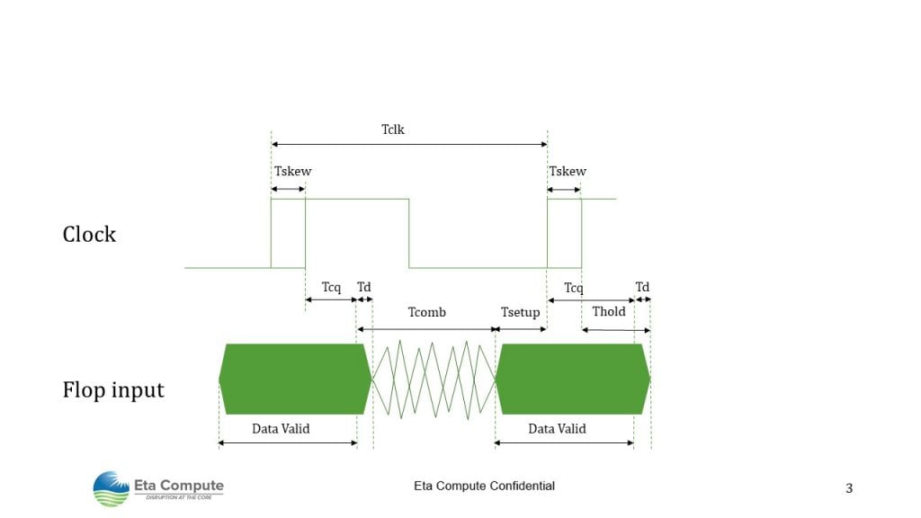
Traditional synchronous MCU and MPUs: Traditional MCU/MPUs are fully synchronous and execute all operations in the device related to an internal clock. At the heart of the device is combinationallogic, and all logic operation must complete within one clock cycle and comply with the setup and hold time of flip flops. When the clock has some skew over the circuit, it reduces the maximum clock period (Figure 1).

The following formulas express this relationship:
Tcomb < Tclk -Tsetup – Tcq -Tskew(1)
Td > Thold + Tskew – Tcq (2)
With Tcomb the time for the combinatory path to provide valid data, Td the time for the combinatory output to start changing, Tclk the clock period, Tskew the clock skew, Tsetup and Thold the minimum setup and hold time for a flip flop, Tcq the launch flop delay from clock to data output.
Tcomb, Tsetup, Thold, Tskew, Tcq, Td vary with voltage, temperature, and manufacturing variations. When designers simulate their circuit, they want to confirm that all combinatory paths comply with (1) and (2) over every condition. Designers call this operation “closing the timing.”
DVFS: Dynamic Voltage Frequency Scaling
In traditional MCU and MPUs, the logic voltage has a significant impact on propagation speed and timing. Designers use a fixed “core” voltage, usually 0.9V to 1.2V depending on the technology and the frequency they want to reach.
When they want to reduce power, one option is to lower the voltage. Indeed, the dynamic power consumption in synchronous circuits mainly consists of switching losses and is proportional to the square of the voltage.
The following formula captures this relationship: Pcpu = Ceff × VDD2 × fSW + Pleak
With Pcpu, the CPU power, Ceff the equivalent effective capacitance of the circuit, VDDthe voltage, fSW the frequency of the circuit, and Pleak the power leakage of the circuit.
Reducing voltage thus reduces power by a quadratic factor and is very advantageous. The drawback is that, however, by reducing voltage, we also reduce the maximum frequency.
If the device can control voltage and frequency together, then a variable voltage scheme can be implemented where voltage varies dynamically with frequency, and this is called Dynamic Voltage Frequency Scaling or DVFS.
The problem is that in a fully synchronous design, the voltage influence on timing is device dependent, and when varying the voltage, the device to device variation increases a lot, and it becomes very challenging to close the timings.
This variability has limited the application and the impact of voltage frequency scaling in traditional circuits: DVFS is usually limited to a small voltage range, a few hundred mV, and to a few pre-defined discrete voltage levels.
A novel approach to power: self-timed CVFS (continuous voltage and frequency scaling)
Eta Compute looked at the problem differently. What if each device could adapt itself to these variations and adjust voltage and frequency automatically?
This is the idea behind our patented technology, the continuous voltage and frequency scaling, or CVFS. In CVFS, the logic is self-timed, adjusting core voltage and clock frequency automatically, ensuring no timing violation. This allows us to modulate frequency and voltage continuously, from the lowest to the highest internal voltage, and always run the most efficient way for a given workload.
CVFS ensures the lowest power operation over a wide voltage range, over the full temperature range and manufacturing variation.
Multicore hybrid architecture
To design a neural sensor processor, we looked at the needs of a complete intelligent IoT node.
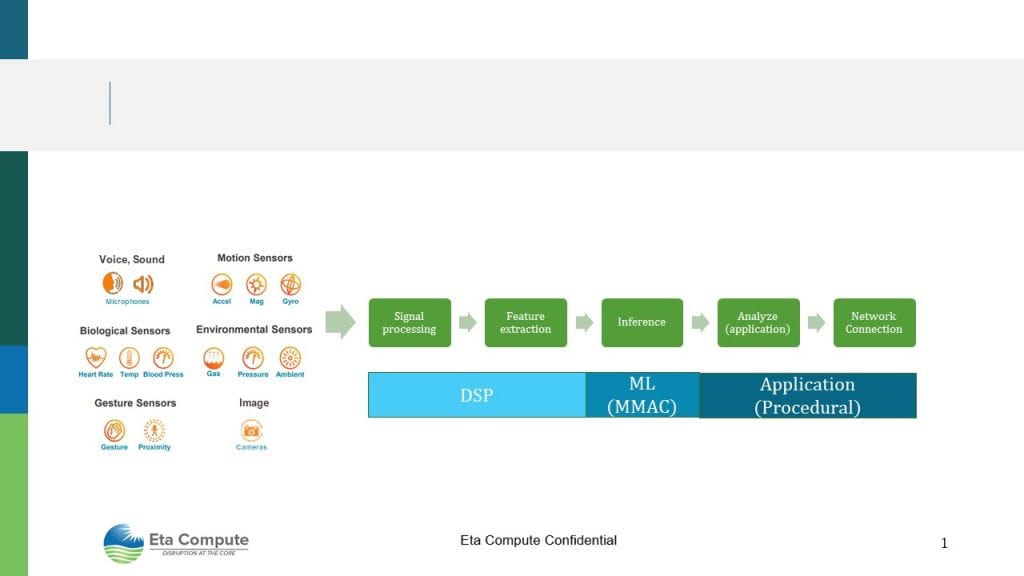
A smart IoT node needs to acquire data from a sensor, do some signal processing and feature extraction, then run a machine learning algorithm. The application then analyzes the inference, and if needed, the connection is established with the network to communicate with the cloud (Figure 2).
IoT nodes require a unique combination of three compute workloads: procedural programming, DSP, and MAC acceleration. The best architecture is a multicore one, and at Eta Compute, we combined an Arm Cortex-M CPU for the procedural load with a dual MAC 16bit DSP for signal processing and MAC accelerations.
Our choice was to design an MCU architecture that brings the integration with analog, power management, and memory, instead of focusing solely on the neural network accelerator.
In the end, this is a very versatile and scalable architecture. It brings the best of both MCU and DSP world and allows us to address any workload in any combination: network stacks, RTOS, digital filters, time-frequency conversions, RNN, CNN, and traditional artificial intelligence like searches, decision trees, and linear regression.
The power advantage of multicore
Having the right core for the right workload as a multiplying effect on the power efficiency. DSPs are more efficient than CPUs for signal processing tasks. It is little know that they accelerate machine learning tasks as well.
Deep neural networks are a pipeline of operations where operands circulate top to bottom. For instance, here are the representations of three popular types of deep neural networks: CNN, GRU and LSTM (Figure 3).
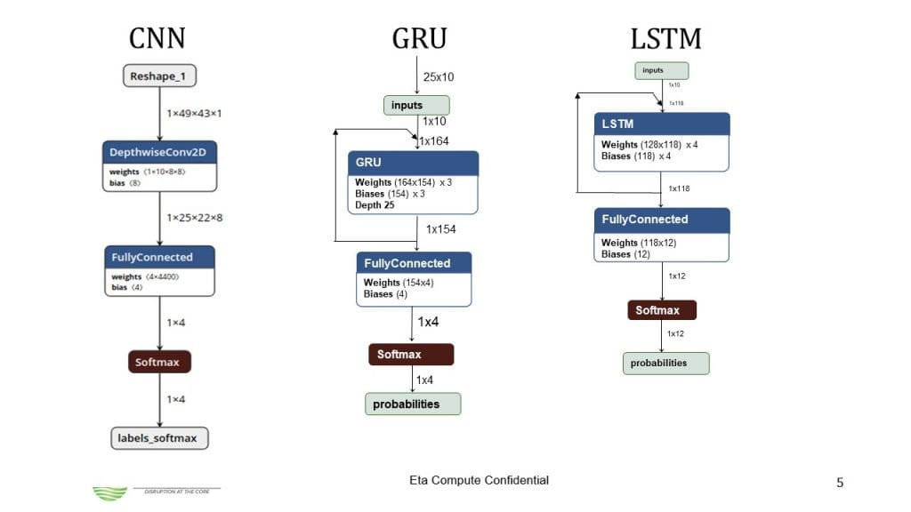
The most cycle intensive operation in these networks is the matrix multiplication that is at the center of the fully connected layer, the convolution and the GRU and LSTM operations. Translated in processor operation, matrix multiply makes heavy use of multiply accumulate or MAC.
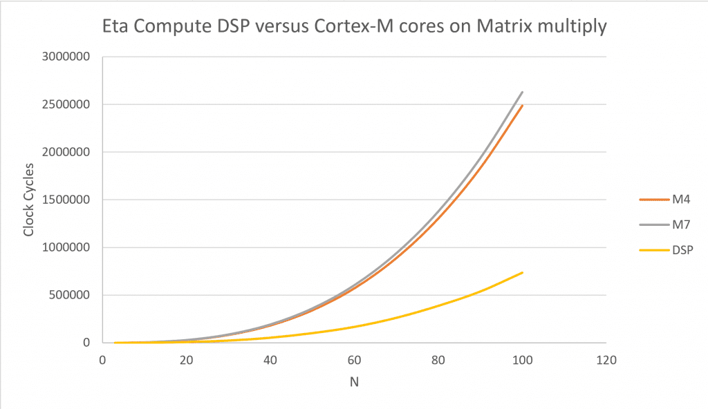
In our case, the DSP we chose is a dual MAC DSP able to execute two 16×16 MACs in one cycle. Moreover, it benefits from the inherent architecture advantages of DSP for calculation: dual memory banks, zero loop overhead, complex address generation. This means it is 2 to 3 times more efficient than an MCU at neural network calculation, as show on the graph in Figure 4.

This 3x advantage is magnified by the multicore approach with CVFS. Indeed, in a multicore architecture, the frequency of each core is a fraction of the frequency of an equivalent single core. Because with CVFS voltage decreases with frequency, having a multicore has a double benefit:
- Better efficiency of the specialized core
- Lower frequency, thus lower voltage and quadratic gain on power for a given workload
At the end, the advantage of a multicore hybrid architecture with CFVS is an additional 10x gain on the device power efficiency.
Production grade neural sensor processor
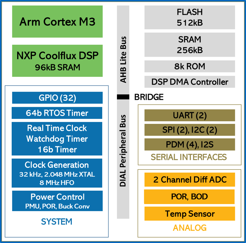
The ECM3532 (Figure 5) is our production-grade neural sensor processor. ECM3532 is a system on chip (SoC) realized with an Arm Cortex-M3 processor, an NXP CoolFlux DSP, 512KB of Flash, 352KB of SRAM, and supporting peripherals.

ECM3532 is implemented using Eta Compute’s proprietary CVFS (Continuous Voltage Frequency Scaling) technology, with dynamic voltage and frequency scaling and near threshold voltage operation.
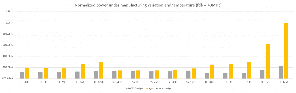
Our design approach accommodates for process and temperature variation much better than the traditional synchronous approach. For instance, the figure below shows power consumption for the Cortex core under various process variations (corner lots) and temperature. Our power consumption at 40MHz does not vary much across process corners and temperature, compared to a standard design that shows a fivefold variation as shown on the normalized graph in Figure 6.

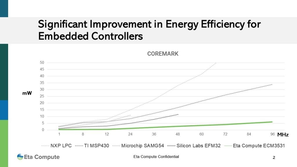
For the cortex only, we are up to 10 times lower power than competitive devices at any given frequency, as shown on the mW per MHz plot of various processors running Coremark (Figure 7).
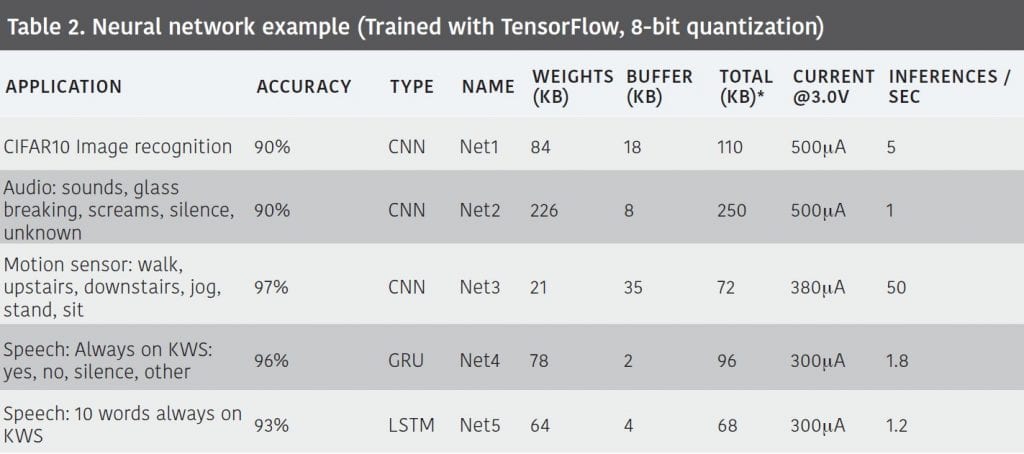
Our processor shines even more when running neural networks. We implemented five types of neural networks for voice, sound, activity and image. In each case, our current consumption is less than 1mA, as shown in Table 2.

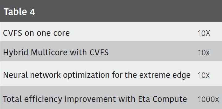
From 10x to 1000x
For a given hardware architecture, Eta Compute’s CVFS allows to reduce power in the order of 10x, as we have seen above. The multicore architecture adds an additional 10x factor, thanks to lower frequency and more efficient cores. We are already at 100x, but at Eta Compute, we believe we can do more.
Developing neural networks for embedded devices is complex, as it requires excellent embedded and AI skills to optimize the network and the overall power consumption. Often, the published neural networks are not designed for extreme edge devices, and proper neural network optimization and software design can achieve a 10X improvement over less careful implementations. There are various design techniques and optimization that we are developing internally and with partners and that improve neural network efficiency dramatically. Our experiments with CNN particularly have shown that we can reduce neural networks size and improve their efficiency by a factor of 10x.
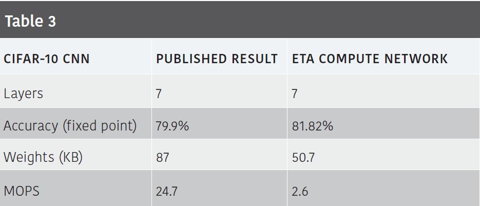
For instance, we optimized a CNN for the CIFAR-10 dataset. Compared with the published academic result (Lai et al, “CMSIS-NN: Efficient Neural Network Kernels for Arm Cortex-M CPUs” [3]) we were able to divide the operations by 10 and the weight size by 2, with similar accuracy, as shown in Table 3.

With this additional technological improvement, we can bring a total 1000X efficiency improvement compared to a direct implementation of neural networks on a standard microcontroller (Table 4).

Scaling intelligence everywhere: software is next
Eta Compute’s vision is to scale intelligence everywhere in the smallest embedded devices and make AIoT a reality. With CVFS and our production device, ECM3532, we have solved the hardware issues hindering the wide deployment of AI at the extreme edge.
CVFS is very scalable: it works the same in any node, with any foundry and any process technology. Even in “Ultra Low Leakage” or “Ultra Low Power” process technologies, it brings a 5 to 10-fold reduction in power. Adding the benefit of our multicore architecture, and the neural network optimization that we can perform, and we are close to a 1000 gain in efficiency. This technology will enable sensors intelligence, augment battery-operated and energy harvested applications with AI, and bring deep learning inference in all IoT devices.
The next step is overcoming the software complexity in implementing neural networks in small devices. Eta Compute is inventing a novel approach to software development that accelerates the development of production-grade deep-learning on embedded applications, taking full advantage of our multicore processors with CVFS.
References
1. Lu, Z., Pu, H., Wang, F., Hu, Z., & Wang, L. (2017). The Expressive Power of Neural Networks: A View from the Width. Neural Information Processing Systems, 6231-6239
2. IDC IOT DATA prediction: https://www.idc.com/getdoc.jsp?containerId=prUS45213219
3. Lai et al, “CMSIS-NN: Efficient Neural Network Kernels for Arm Cortex-M CPUs”