VAN YANG, EAGLE ZHANG, and AARON HE, Analog Devices, Inc.
Ultrahigh frequency radio frequency identification (UHF RFID) systems have been widely adopted for applications such as asset management and apparel retail. Recently, they have gained attention for use in unmanned supermarket applications and for the electronic identification of motor vehicles. This article focuses on a target application for the electronic identification of motor vehicles in China, which must be compliant with the Chinese standards GB/T 29768-2013 “Information Technology—Radio Frequency Identification—Air Interface Protocol at 800/900 MHz” [1] and GB/T 35786-2017 “General Specification for Read-Write Equipment of the Electronic Identification of Motor Vehicles.” [2] This article describes two implementations, showing how engineers can trade off receiver sensitivity for reduced design complexity, component count, and board space. Although the RF front end described in this article is application specific, both the analysis method and the front end itself are applicable for general UHF RFID reader solutions.
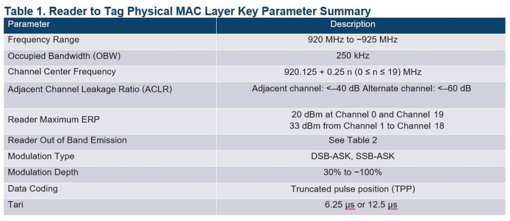
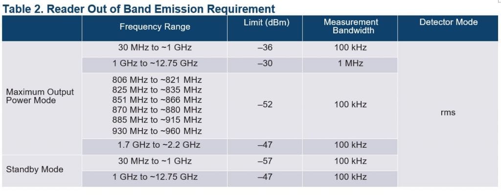
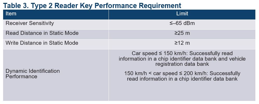
Standards summary
According to the GB/T 29768-2013 and GB/T 35786-2017 standards relating to the electronic identification of motor vehicles, the key air interface parameters and the performance requirements of high performance Type 2 readers for these applications are summarized in Table 1 through Table 3.


System link budget analysis
Passive RFID systems have two fundamental link limits: The forward link normally limited by the minimum RF to dc power to supply the tag electronics and the reverse link limited by the reader receiver sensitivity. The forward and reverse link budget formulas [3,4] are described in Equation 1 through Equation 3:

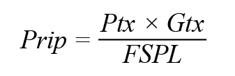

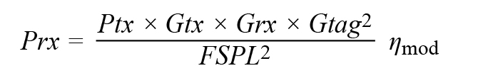

Prip: tag receive isotropic power
Ptx: reader transmit power
Gtx: reader transmit antenna gain
Gtag: tag antenna gain
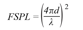
FSPL: free space pass loss
Prx: reader receive signal power
Grx: reader receive antenna gain
ƞmod: tag modulation efficiency
d: distance between reader and tag
λ: signal wavelength in free space
As defined in GB/T 35786-2017 section 6.2 and section 6.5.2.2, Ptx is 30 dBm and the feeder cable insertion loss is less than 1 dB, so the real Ptx is around 29 dBm. An antenna of 10 dBi to 12 dBi gain is used in the field test, so Gtx is assumed to be 12 dBi. As for Grx, in an electronic identification of motor vehicles application, the reader normally uses the monostatic configuration, whereas a single antenna is used at the reader for both transmission and reception, so Grx = Gtx = 12 dBi. A tag antenna is usually similar to a dipole and it is reasonable to assume Gtag = 2 dBi. ƞmod represents the modulation efficiency of the tag, which depends on the tag antenna matching and the tag impedance shift that occurs during modulation and it is reasonable to assume that ƞmod = –8 dB. The center frequency is 922.5 MHz, so λ = 0.33 m. The system link budget shown in FIGURE 1 is based on the previously described formulas and parameters.

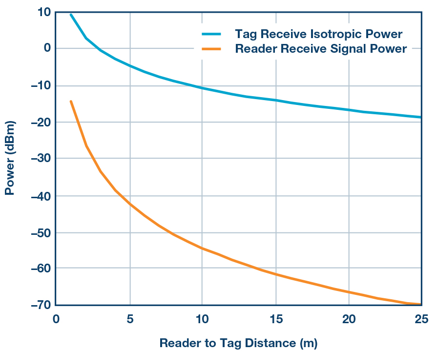
To support the link range at 25 meters as defined in the standard, the tag sensitivity should be better than –18.7 dBm and the reader sensitivity should be better than –70.4 dBm. In the standard, the tag sensitivity requirement is defined as –18 dBm, which matches the analysis result quite well. However, the reader sensitivity requirement is defined as –65 dBm, which has considerable deviation when compared to the analysis result. This deviation may come from the tag antenna gain value. In electronic identification of motor vehicles applications, it is not necessary to design the tag antenna to be omnidirectional. Adding a reflector will result in an additional 3 dB antenna gain. And since the tag antenna gain (Gtag) is squared in Equation 2, the reader sensitivity analysis result will increase by 6 dB to be at –64.4 dBm. In this case, the analysis result will match with the standard requirement.
Self jammers in UHF RFID readers
In a UHF RFID system, the reader transmits a continuous wave (CW) signal to power the passive tags while simultaneously receiving the backscattered signal from the tag at the same frequency. Due to the poor transmitter-to-receiver isolation, the strong CW signal, together with the related transmitter noise, will leak into the receiver. Usually this leakage signal is called a self jammer (SJ) signal and this self jammer signal will degrade the reader’s sensitivity.
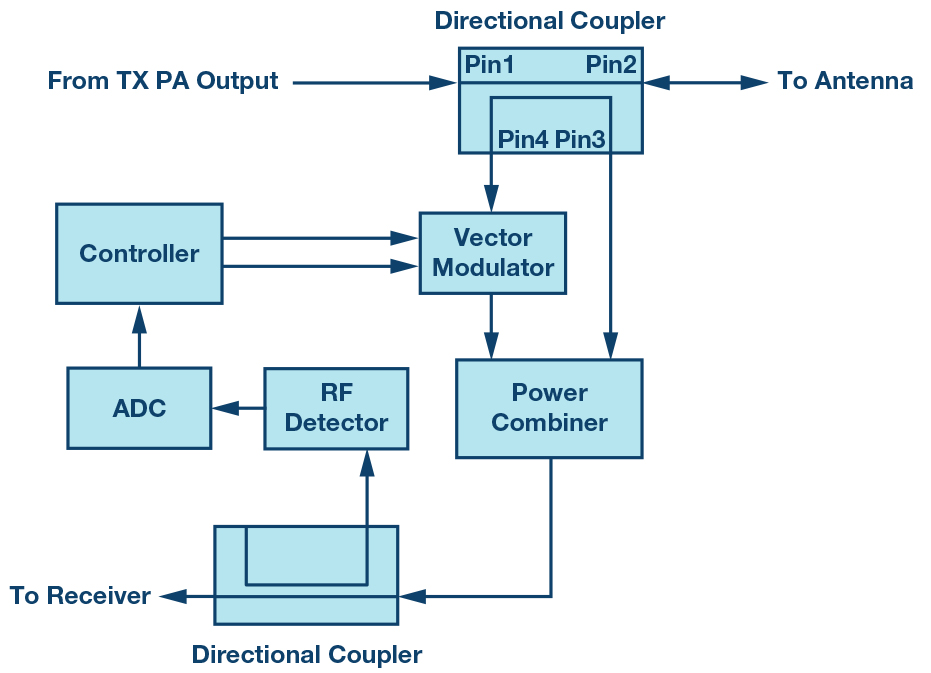
In an RFID reader for the electronic identification of motor vehicles, a directional coupler is normally used as the duplexer for the transmitter and receiver. The SJ signal occurs mainly because of the reflection of the antenna, the limited isolation of a directional coupler, and the reflection of the circuit connected to the coupler port.
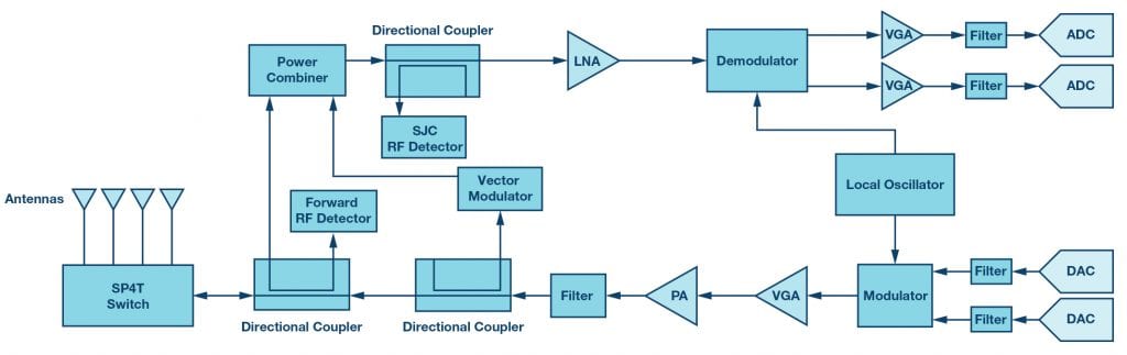
To overcome this SJ signal issue, two methods could be used. The first one is to design a self jammer cancellation (SJC) circuit before the receiver LNA. The second method is to use direct conversion receiver architecture while using the same local oscillator (LO) that’s used by the transmitter and the receiver. In this case, the self jammer signal will convert to dc at baseband, and then dc block capacitors will be used for the ac coupling of the signal. After this dc blocking point, the SJ signal is removed and the dynamic range requirement on the subsequent components is loosened. This means that enough gain could put on baseband to decrease the receiver noise figure (NF). These two methods could be used separately or combined. A typical SJC circuit is shown in FIGURE 2. [5]

Reader key RF performance analysis
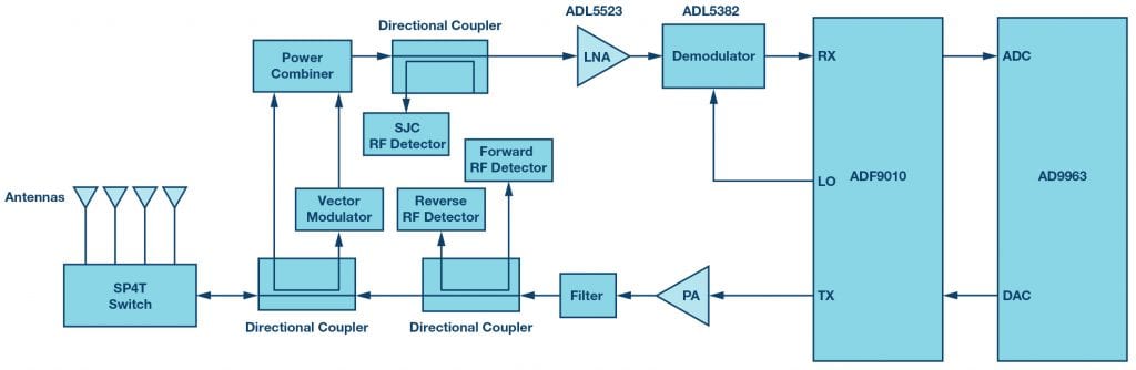
An SJC circuit including a UHF RFID reader RF front-end block diagram is shown in Figure 3. Analog Devices’ AD9963 integrates a dual-channel DAC and a dual-channel ADC. ADF9010 integrates a transmitter modulator, PLL/VCO, and receiver baseband filter and PGA. The demodulator ADL5382 is included on the ADF9010 evaluation board. The ADL5523 is used as an LNA as it provides low noise figures, high gain, and high linearity. The 75 dB high dynamic range RF detector LT5538 is suitable for the SJC RF power detector.

For the transmitter, in the digital domain, the signal should be low-pass filtered to meet both the frequency domain ACLR requirement and the time domain RF envelope requirement. And in the analog domain, both PA linearity and LO phase noise will impact the ACLR performance. The low-pass filtered, TPP coded ASK signal has around a 2 dB peak-to-average ratio (PAR). The average PA output power is around 32 dBm, with a 1 dB margin, so a PA of more than 35 dBm P–1 dB should be chosen. As for the LO phase noise, the phase noise integration from 125 kHz to 375 kHz should be less than –40 dBc and the phase noise integration from 375 kHz to 625 kHz should be less than –60 dBc. As for the out of band emission requirement, an RF filter is needed to meet the requirement at the transmitter harmonics frequency. For the requirement close to working frequency such as the requirement of –52 dBm of 100 kHz measurement bandwidth at 915 MHz and 930 MHz, the RF filter normally has no attenuation yet, so the noise floor requirement for the modulator at 0 dBm output power is around –52 – 10 × log10 (105) – 30 = –132 dBm/Hz. And the phase noise requirement at a 5 MHz offset should be less than –132 dBc as well.
For the receiver, the receiver sensitivity is specified as –65 dBm in the GB/T 35786-2017 standard. It is assumed that the reader should meet this –65 dBm sensitivity at all possible data rates and that the back link frequency (BLF) of 640 kHz is the worst case. For an SJC that includes an RFID reader, the insertion loss from an antenna port to the SJC output is around 15 dB, so that the sensitivity requirement at the SJC output point is –80 dBm and assume the tag backscattered signal power not including dc is –80
– 3 = –83 dBm. The ASK modulation signal demodulation threshold is around 11 dB and the signal bandwidth of BLF 640 kHz uplink signal is 2.56 MHz. So the total NF requirement is NF ≤ –83 – (–174 + 10 × log10 (2.56 × 10⁶) + 11) = 15.9 dB. This total NF requirement includes the impact of the noise of the receiver circuit after SJC, the SJC circuit induced noise, and the transmitter leakage noise. Assuming the delay is matched between the vector modulator signal branch and self jammer branch, which means both the CW self jammer signal and the transmitter leakage noise are cancelled. The transmitter leakage noise includes three parts: the phase noise, the amplitude noise, and the white noise. Normally the amplitude noise and the white noise will be cancelled to the noise floor of –174 dBm/Hz. For the residual phase noise, since the transmitter and receiver use the same LO, it will convert to dc during down conversion because of the range correlation effect. [6] In this case, the vector modulator branch noise will be the only extra induced noise. Assume the vector modulator branch noise floor is –162 dBm/Hz, so at the SJC circuit output, the effective NF is –174 – (–162) = 12 dB, then the NF requirement for the receiver circuit after SJC is 10 × log10 (101.59 – 101.2) = 13.6 dB.
Receiver sensitivity
This first implementation takes a two-chip approach that focuses on receiver sensitivity combining an RF transmitter with converter. Specifically, the ADF9010 is a fully integrated RF transmitter modulator, local oscillator (LO), and receiver analog baseband front end that operates in the frequency range of 840 MHz to 960 MHz. The AD9963 is a 12-bit, low power MxFE® converter that provides two ADC channels with sample rates of 100 MSPS and two DAC channels with sample rates to 170 MSPS. Figure 4 shows the block diagram for the UHF RFID reader RF front end\. The NF of the ADL5523 cascaded with the ADL5382 and ADF9010 receiver gain setting of 24 dB is less than 3 dB.

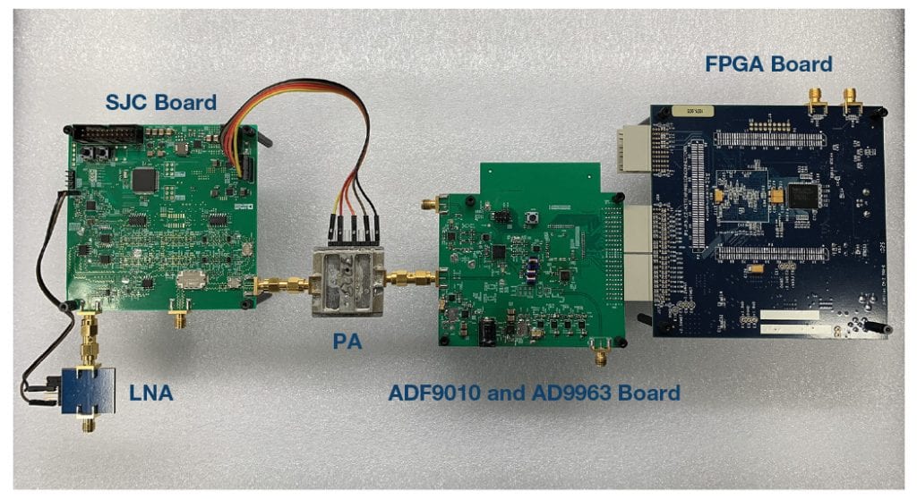
To implement the UHF RFID reader RF front end, both an SJC board including the adaptive SJC algorithm and the ADF9010 and AD9963 board are built. The ADF9010 and AD9963 board integrated the demodulator ADL5382 as well. The two boards are cascaded to test the transmit and receive system-level RF performance.
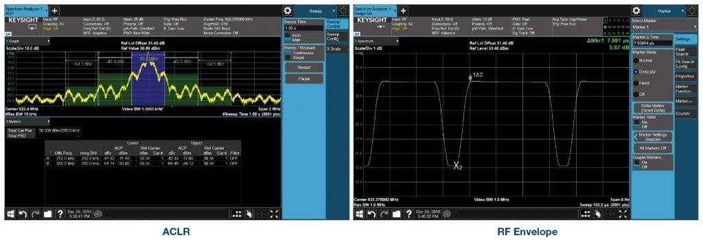
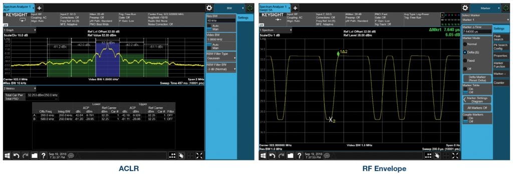
For the transmit test, a TPP coded, 50% modulation depth, DSB-ASK with Tari set to 12.5 μs RFID downlink waveform is built in Python® and downloaded to the FPGA board. The spectrum domain ACLR and time domain RF envelope are tested at the antenna port with a PA output power of 32 dBm. The test setup is shown in Figure 5. For the ACLR test result, the adjacent channel is around –42 dBc which has 2 dB margin and the alternate channel is –64 dBc which has a 4 dB margin. For the RF envelope, the ripple is less than 1%, which has enough margin when compared to the 5% limit and the rise time and fall time are in the range limit of 1 μs and 8.25 μs.

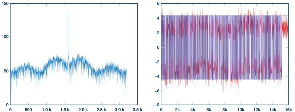
For the receive test, a Tag simulator is built using the Analog Devices SPDT RF switch HMC545A and it is controlled by a microcontroller unit. The control pattern is an RFID uplink FM0 coded data list. An ASK decoding program is built by MATLAB.® By using this program to decode the IQ and comparing it to the original data in the data list, the BER and the receiver sensitivity can be calculated. Figure 6 shows the received IQ data and the FFT plot. Figure 7 shows that a –74 dBm RFID uplink signal with 320 kHz BLF was successfully decoded by the program.


Reducing design complexity, component count, and board space
For some applications, engineers may have the option to choose to trade off receiver sensitivity for design complexity, component count, and board space. In these cases, a more integrated RF transceiver like the AD9361 can be used that integrates all RF, mixed-signal, and digital blocks necessary to provide all transceiver functions in a single device. To implement a UHF RFID reader, the transmitter and receiver should use the same LO to take advantage of the range correlation effect, so the AD9361 transmitter monitor path, rather than the normal receiver path, will be used. The transmitter monitor path bypasses the internal LNA, so an external LNA, such as the Analog Devices ADL5523, is added. The ADL5523 is a high performance GaAs pHEMT LNA with 0.8 dB NF and 21.5 dB gain. The block diagram in Figure 8 shows the implementation of the UHF RFID reader RF front end. Compared to the discrete component implementation (Figure 4), this approach is significantly simplified. The AD9361 baseband is dc coupling, rather than ac coupling. In this case, it is required that the SJC circuit can decrease the self jammer signal to a low enough level—for example, less than –35 dBm—that will not saturate the analog circuit. This allows the self jammer converted dc signal to be removed in the digital domain.

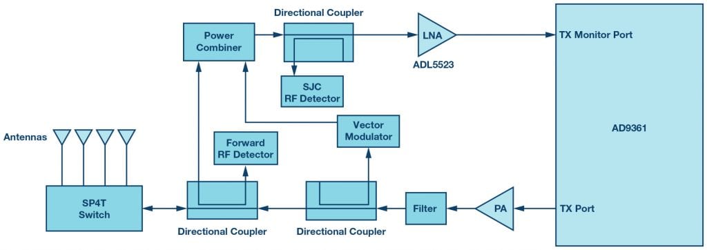
The AD9361 transmitter monitor path gain distribution is comprised of two gains: front-end gain (transmitter monitor gain) and receive low-pass filter gain (GBBF). The transmitter monitor gain could be set to 0 dB, 6 dB, or 9.5 dB. GBBF could be set from 0 dB to 24 dB with 1 dB step. With this flexible gain configuration, receiver AGC functionality could be implemented easily. For this UHF RFID reader application, a transmitter monitor gain setting of 3 dB and a GBBF setting of 6 dB is chosen. When the AD9361 gain setting is 3 dB, then the cascaded NF of the ADL5523 and AD9361’s transmitter monitor port is around 12.6 dB. This setting has a 1 dB margin compared to the analysis requirement of 13.6 dB, while the digital domain power is –7 dBfs if the residual self jammer is –35 dBm.
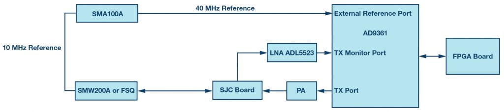
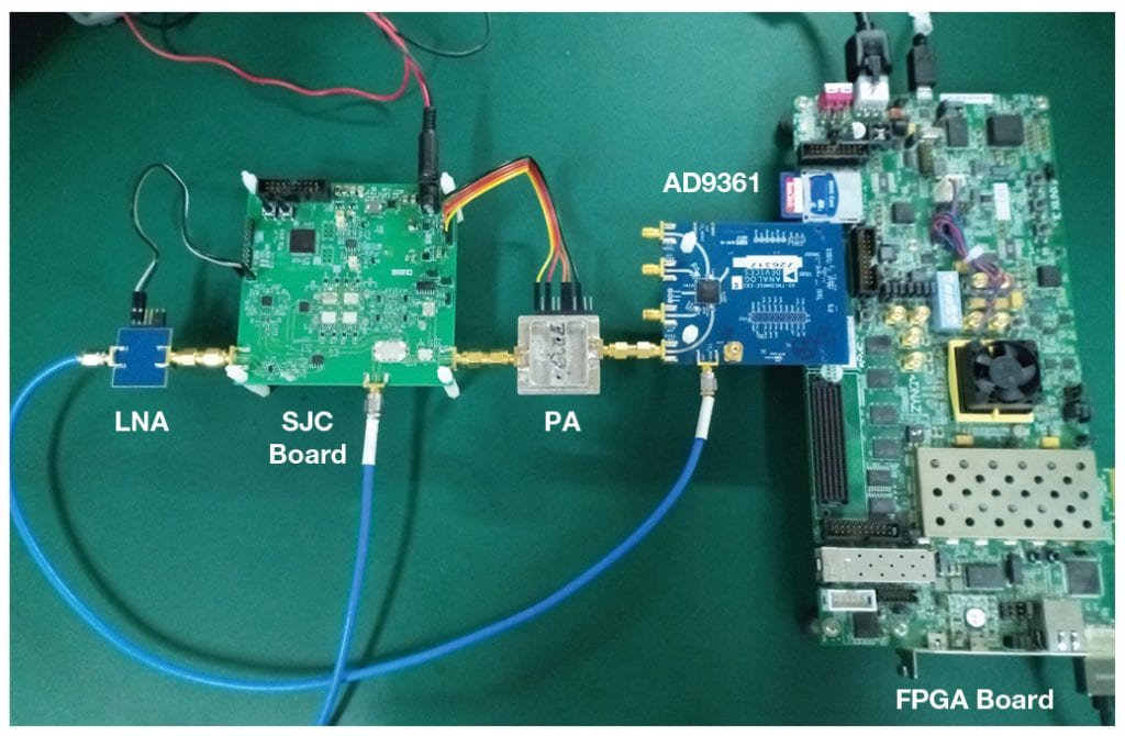
To implement the UHF RFID reader RF front end, an SJC board including an adaptive SJC algorithm is built. This is cascaded with AD9361 to test transmitter and receiver system-level RF performance. The test setup block diagram and photo are shown in Figure 9 and Figure 10.


The test result is shown in Figure 11. For the ACLR test result, the adjacent channel is around –42 dBc, which has a 2 dB margin, and the alternate channel is –61 dBc, which has a 1 dB margin. For the RF envelope, the ripple is less than 1%, which meets the margin requirements for a 5% limit. The rise time and fall time are in the range limits of 1 μs and 8.25 μs.

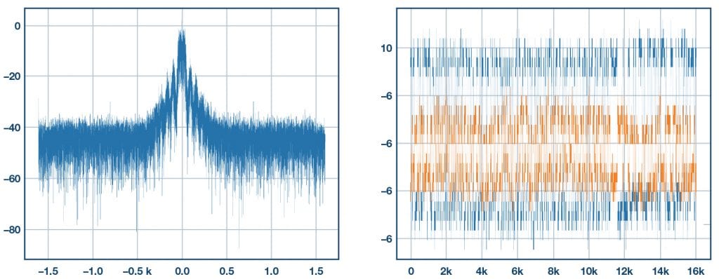
For the receiver test, an RFID uplink FM0 coded data list is built and downloaded to the signal generator SMW200A and then configured for SMW200A to transmit a DSB ASK signal with this data list. The AD9361 received IQ data are stored in the FPGA board and fetched to a PC using an FTP tool. An ASK decoding program is built by MATLAB. Using this program, decoded data is compared to the original data in the data list, which then allows for the BER and receiver sensitivity to be calculated. Figure 12 shows the FFT plot and decoded data of the MATLAB program. It is tested that –65 dBm RFID uplink signal with a 640 kHz BLF is successfully decoded by the program.

Engineers have many options when designing a UHF RFID reader RF front end. For applications that need high receiver sensitivity, a discrete implementation provides better results. For other applications, an integrated approach balances the trade-off of receiver sensitivity degradation with a greatly simplified design, lower component count, and reduced board space. Although the RF front end described in this article is application specific, both the analysis method and this front end itself are applicable for general UHF RFID reader solution.
References
1.GB/T 29768-2013 “Information Technology—Radio Frequency Identification—Air Interface Protocol at 800/900 MHz.”
2. GB/T 35786-2017 “General Specification for Read-Write Equipment of the Electronic Identification of Motor Vehicles.”
3. Monza X Antenna Application Note. Impinj.
4. Gregor Lasser and Christoph F. Mecklenbrauker. “Self-Interference Noise Limitations of RFID Reader.” 2015 IEEE International Conference on RFID (RFID), June 2015.
5. Alírio Boaventura,João Santos, Arnaldo Oliveira, and Nuno Borges Carvalho. “Perfect Isolation: Dealing with Self-Jamming in Passive RFID Systems.” IEEE Microwave Magazine, Vol. 17, No. 11, November 2016.
6. Byung-Jun Jang and Hyun-Goo Yoon. “Range Correlation Effect on the Phase Noise of an UHF RFID Reader.” IEEE Microwave and Wireless Components Letters, January 2009.
About the Authors
Van Yang is a system applications engineer manager at ADI Shanghai. Van joined ADI in 2015 as an FAE for industrial and healthcare customers support. Prior to joining ADI, Van worked as an FAE at TI for over four years. He graduated from Huazhong University of Science and Technology with a master’s degree in communication and information systems. He can be reached at van.yang@analog.com.
Eagle Zhang is a field applications manager at ADI Shenzhen. Eagle joined ADI in 2001. He started his role as field applications engineer at ADI, and then worked as an ADI China core market technical support manager and ADI southern China field applications manager. During his time as a field applications manager, Eagle built the ADI southern China field technical support team. Eagle earned his bachelor’s degree and master’s degree in engineering thermal physics from Tsinghua University. He can be reached at eagle.zhang@analog.com.
Aaron He is a system applications engineer at ADI Shanghai. Aaron joined ADI in 2017. Prior to joining ADI, Aaron worked as a senior RF engineer at Ericsson. He has more than 10 years of experience working on wireless communication base station design, integration, and production test system development. Aaron received his B.S. in telecommunication engineering from Xi’an Jiaotong University in 2001, and his M.S. in microwave engineering from Huazhong University of Science and Technology in 2006. He can be reached at aaron.he@analog.com.