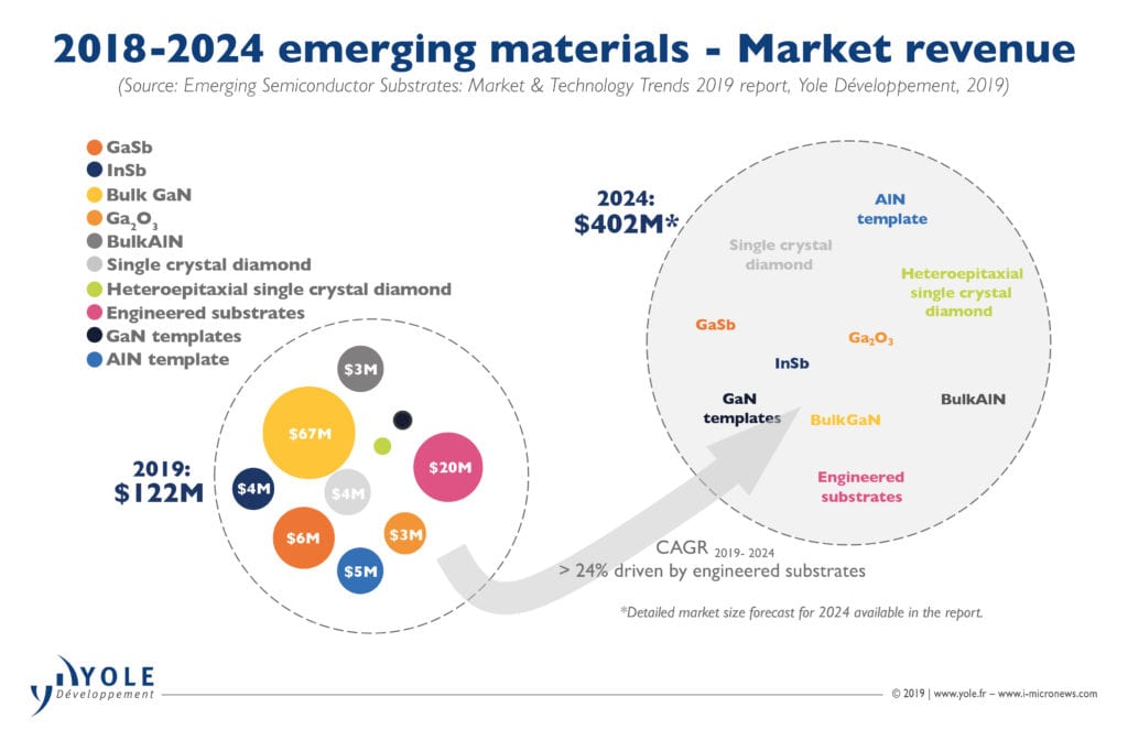
The silicon world is not perfect. It is a fact. Industrial companies are daily trying to push this substrate beyond its limits. Under this context, alternative platforms and compound semiconductors have emerged and the semiconductor industry is showing today lot of success stories: GaAs for RF and photonics applications, SiC for power and RF applications, GaN -on-sapphire for LEDs , and SOI for RF and CIS imaging sensors and more. Without doubts, electronics and photonics applications are creating plenty of opportunities for emerging semiconductor substrates. Combined, Yole Développement (Yole) expects the emerging semiconductor substrate market to surpass US$400 million, growing at a 24% CAGR between 2018 and 2024.

The market research and strategy consulting company, Yole proposes today a comprehensive technology & market report focused on the emerging semiconductor substrates. Emerging Semiconductor Substrates: Market & Technology Trends report covers state-of-the-art crystalline semiconductor substrates, including GaSb , InSb , GaN, Ga2O3 , AlN , and diamond. GaN, AlN templates, and engineered substrates like POI are also well detailed in this market & technology analysis. The emerging semiconductor substrates report conveys Yole Développement’s (Yole) understanding of these substrates’ application potential in RF, power electronics, photonics (including laser diodes), LEDs, sensors, and detectors.
This report is part of Yole’s global strategy to propose a deep understanding of the overall semiconductor supply chain and its evolution. From emerging semiconductor substrates to UV LED or EEL, including RF components for 5G for example, analysts are daily interacting with leading companies to understand technical issues and market challenges. With a special focus on emerging substrates, Yole’s analysts point out today opportunities of business and development for emerging substrates and related products.
Starting with RF applications, there are numerous market drivers, including 5G for infrastructure and handsets, defense applications and civil automotive radar, and more. For example, 5G deploys MIMO , which is used in high-end 4G LTE phones. MIMO is obligatory for handsets, and more filters will be needed. Plus, better performance is required, which implies a big market opportunity for new materials.
Under this context, Yole’s analysts had the opportunity to exchange with Christophe Didier, Manager, Filter Business Unit at, Soitec, the leader in designing and manufacturing innovative semiconductor materials. Analysts and Christophe Didier debates about engineered substrates, related applications and technical issues. Discover the full interview on i-micronews.com: Engineered substrates for filters is taking off (Published on May 23).
“From a power electronics perspective, which is currently driven by the electrification of transportation, renewable energy, motor drive, and numerous power supply applications, enhanced device performance to reduce power consumption is a general trend,” comments Hong Lin, PhD. Senior Technology & Market Analyst at Yole; “And this evolution has created numerous market opportunities for WBG materials like SiC. Indeed, the SiC power device market is taking off, though the substrate remains expensive.”
The photonics market, ranging from UV to the IR spectrum also brings significant opportunities: from water purification and gas sensors, to infrared imagers. Since the wavelength is determined by the bandgap of the material, which is intrinsic to each material, different materials are being developed to push the wavelength towards shorter or longer regions.
“There are many drivers to push emerging materials,” asserts Ezgi Dogmus, PhD. Technology & Market Analyst at Yole. “Researchers and engineers have plenty of ideas”.
Starting with GaSb and InSb LDs and PDs based on these materials are already deployed in performance-driven military applications. But this is not all. For example, IQE, a leading antimonide wafer and epiwafer supplier, is actively engaged with tier1 OEMs on new opportunities to migrate antimonide-based “see in the dark” IR technologies into consumer markets.
Yole also sees that an emerging GaSb-based type-2-superlattice (T2SL) technology is being developed by several major detector players including FLIR, Semiconductor Devices, and IRnova. This technology is expected to penetrate into consumer applications, with ramp-up in the coming years.
Bulk GaN wafers have for many years been widely used for laser diode applications. Recently, researchers have explored their usage in power electronics and RF applications. Yole’s analysts see a growing effort, led by Japanese players, ranging from materials suppliers to device suppliers like Toyoda Gosei, to make vertical GaN-on-GaN power devices happen.
In the meantime, an ultra-wide band gap material (Ga2O3) is garnering increased attention. Wafers up to six inches have been demonstrated, with the promise of potentially lower cost than today’s SiC solutions. Future ramp-up will depend on technology/cost competition from other existing solutions.
“Up to now we have considered bulk crystal materials, but they are not the whole story,” concludes Ezgi Dogmus from Yole. “Templates and engineered substrates are also being developed for either lower cost (i.e. SiC and poly SiC bonding) or better performance, such as piezo-on-insulator for filter applications…”