This article is the second part of a two-part special on advancements in EUV lithography. Click here for Part 1: EUV Lithography: Weighing the Options for Future Logic and Memory Applications
Manufacturing the chips for your smartphone or laptop involves a great number of process steps. The most challenging one is probably lithography, in which the circuit elements are printed in silicon. With features becoming smaller and process steps becoming more complicated, chip makers are looking to extreme ultraviolet (EUV) for the answer. And indeed, the technique is viewed as essential for the future of high-volume semiconductor manufacturing. But that doesn’t mean the road beyond 7nm is wide open. Stochastic effects remain the major roadblock.
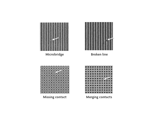
Stochastic printing failures are random, non-repeating, isolated defects such as microbridges, locally broken lines and missing or merging contacts (Figure 1). They are believed to arise from the fundamental relationship between energy and wavelength. With the wavelength getting shorter – EUV lithography operates at 13.5nm – the energy from the light source is distributed over less photons. Consequently, there are just a few photons to create a pattern. Besides this so-called “photon shot-noise effect”, stochastic effects originate from the molecular nature of matter, and the probabilistic behavior of their interactions. Stochastics have been plaguing EUV lithography for years and have been the topic of many papers and talks. Philippe Leray, group leader of the litho process and pattern control group, and Peter De Bisschop, senior scientist in the imaging and reticles team, shed light on the latest developments in imec to detect, understand and mitigate stochastic failures.

Looking for the broken needle in a waferstack
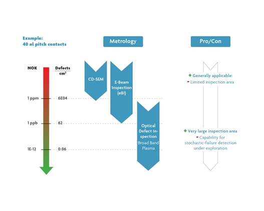
When developing patterning modules for critical layers, it is key to reduce failure probability. That is easier said than done. As we currently don’t have a complete theoretical framework to predict the failures, their density can only be obtained by measuring them from printed wafers —which in turn assumes that we have the metrology to detect them. The stochastic challenge is very pronounced in the inspection capability where we have to strike a balance between speed and sensitivity. Speed, because a large amount of data is necessary to assess the problem; sensitivity, because the failures are usually very small.
The easiest-to-use method is CD-SEM (critical dimension scanning electron microscopy). While it is generally applicable – for both resist and etch wafers and for all types of stochastic failures – it is also area-limited. Because the method depends on the time it takes generate CD-SEM images, a whole wafer would take months to scan. E-beam tools are also SEM-based but can inspect larger areas and find rarer defects. The drawback of this method is that the high-energy electron beam is destructive for the resist and the speed is still not sufficient to scan full dies (or wafers). Many e-beam-companies are therefore exploring multi-e-beam as an answer to the speed-issue. But parallelizing 1000s of beams is no walk in the park; they need to be calibrated and should not interact.
“The ultimate method that everybody wants to use, is optical defect inspection. The advantage of that technique is that you can scan whole wafers, and that’s exactly what the industry needs. It is the go-to method to reach the threshold of detecting 0.01 defect/cm2,” states De Bisschop. The optical inspection field is indeed taking major steps forward with the exploration of new wavelengths and new software capabilities to maximize the signal-to-noise ratio.
The Holy Grail that is optical inspection?
At the same time, the enthusiasm comes with one important caveat: the benefits in using optical inspection only hold if the technique is reliable. To be more concrete, that it can indeed achieve a high capture rate with good signal-to-noise ratio for all types of stochastic failures, on etched wafers and on resist wafers. And whether that is the case, is still an open question. Unlike, for example, CD-SEM which unambiguously shows the printed patterns, optical defect inspection does not show details on the wafer. It detects a color variation in a standard pixel of 50nm and compare it to a point of reference. So, with enough light you can distinguish subtle intensity changes compared to that reference, but you don’t see the actual defect.
Moreover, the fact that optical defect inspection is able to detect very small features might come at a price. Optical techniques have been used traditionally and successfully to find classic defects or particles. And these are large enough. “But now, failures have become so small that we have to ask ourselves whether the optical method has sufficient sensitivity to detect these small stochastic printing failures, such as a single microbridge or one missing contact. Today, this is still largely an open question. On the other hand, for failure-substrate types for which it doeswork well, it will be without a doubt the method of choice,” concludes De Bisschop.
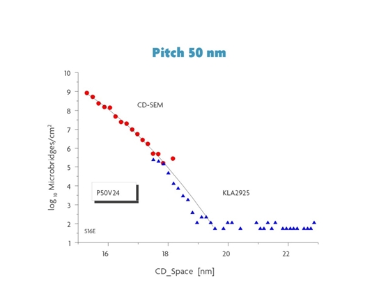
So, we are still missing the one method that can do everything. Each technique has its pros and cons (Figure 2). For example, when comparing optical inspection with CD-SEM for microbridge detection, it shows that they both operate in a different – but complementary – regime. Measuring the high-failure probability range with CD-SEM is not a waste of time, as extrapolating the measured data even a few orders of magnitude, appears to give us a reasonable forecast of the trend. At the same time, we found that optical inspection has excellent sensitivity for stochastic microbridge failures on etched wafers, even though these failures are very small (Figure 3).


The rise of machine learning
Efforts are also ongoing to make existing tools faster – using machine learning. CD-SEM is significantly slower than SEM-Review even though both of them are SEMs using a single beam. The difference is that the first takes very precise measurements in a very small pixel, while the latter takes a quick picture on which to detect a defect. “Of course, when you scan faster, you lose more resolution and thereby the capability of detecting small failures. However, we are playing with the idea of using machine learning techniques such as fast face recognition, to reconstruct a sufficiently high-quality image for failure detection starting from a low-res image. If we could accelerate beam inspection that way, maybe we don’t need 1000 beams, but we can live with 100,” says Philippe Leray.
Another application of machine learning is more oriented towards process control. On the road to an integrated circuit device, a wafer passes through numerous tools, each depending on highly controlled protocols, and thus requiring tight in situ process monitoring. As a side effect, a massive amount of data is created. For example, when looking for a defect, you detect the defect, verify it, and then store the image. Equally, when determining a plasma etch endpoint, you look at the optical spectra of the plasma. Both the images and optical spectra contain far more information than ‘just’ the defect or the endpoint. Leray: “The idea is to collect all this data along the processes of all tools – both process and metrology tools – and teach a machine to look for a pattern in that data. That way the machine might explain the failures, deviating critical dimensions (CDs), or bad etches and connect them to a parameter during the process flow. Even when the pattern is too subtle, too intricate or too correlated for a human to see.”
The stochastic landscape
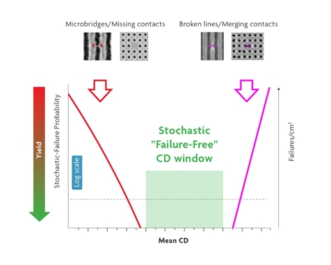
In the end all methods open another window on the ‘stochastic landscape’ that visualizes the dependency of the stochastic failure probability on the printed CD. At the small-CD side, we find a very steep (almost exponential!) increase of the failure probability with decreasing CD. This rapid increase is referred to as the ‘stochastic cliffs’. For dense structures, there are two cliffs: at the small space-CD or contact-CD side there is an exponential increase in microbridges or missing contacts while at large space-CD or contact-CD side the probability for broken lines or merging contacts increases rapidly (Figure 4). For less dense structures, both cliffs exist as well, but only the low-CD patterning cliff poses a practical problem. The cliffs are not the only limiting factor. At this year’s SPIE Advanced Lithography, imec showed for the first time a case where the number of (microbridge) failures never reaches zero, but rather hits a constant ‘floor’. This is an important discovery as it suggests that there might be a second failure mechanism that behaves in a different way.
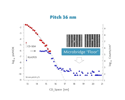
Even though the origins of this floor are still unknown, the repercussions of its existence might be significant. Manufacturable CDs can only be achieved if they are sufficiently far away from the cliffs. And, with denser structures the passage between the cliffs becomes narrower. This is a fundamental problem that the litho-community has to solve. “But the floor adds another dimension to that problem. Sailing away from the cliffs does not necessarily mean that you are also escaping from the floor. In other words, even when you manage to stay away from the cliffs obtained from your measurements, you are still not sure that you will be in failure-free waters,” explains De Bisschop.
Tackling the stochastic challenge
Once we know what the stochastic-failure landscape looks like, we can develop targeted strategies to reduce failure densities. Currently, work towards that goal operates on two fronts: mitigating failures by tweaking parameters and understanding the mechanisms behind the failures.
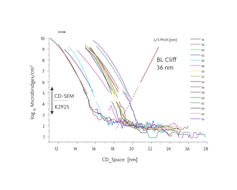
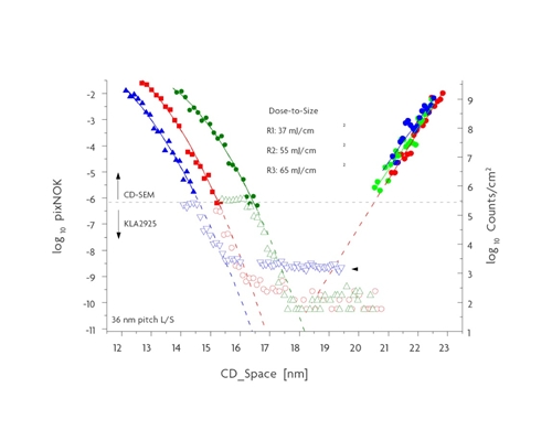
Where exactly the cliffs are, depends on the materials used and on a long list of parameters. You can always toggle the switches, but never entirely eliminate the cliffs. Plus, it is a delicate exercise. In any application featuring different structures, you will always work with different pitches (Figure 5a). Consequently, the combination of all resulting cliffs might silt up the passage entirely. That is also why the use of higher dose resists is increasingly more accepted (Figure 5b). And indeed, it does push back one of the cliffs (the microbridges) but, surprisingly, does not appear to have an effect on the second cliff (the broken-line cliff) nor on the floor. So, it is not a miracle switch.
Not only the dose, but also the resist is an important factor for stochastic-failure performance. Imec has made recent progress in reducing stochastic nano-failures and line roughness by implementing sequential infiltration analysis (SIS), an existing technique, commonly used in directed self-assembly (DSA) and now applied in EUV lithography. During SIS, the photoresist is infiltrated with an inorganic element to make it harder and more robust, thereby enhancing the patterning performance.
“Since there are numerous parameters to play with and each one of them has an effect, there should be ‘an optimal setting’ for each parameter. Most likely, none of the switches can fully eliminate the problem, so every contribution is necessary to find the ultimate combination of parameter settings that is just good enough,” comments De Bisschop. “Basically, we want to develop a recipe in a reasonable time frame. Some tools have a few 100 possible combinations of parameters; too many for a human to explore. This is clearly another field where machine learning could help,” adds Leray.
Learning from failures
Strategies to counter failures would strongly benefit from a better understanding of the mechanisms behind these failures and an increased knowledge of which parameters in the patterning process impact their probabilities.
Because of the short wavelength of EUV, high-energy photons hit the resist, creating complex interactions. A fundamental understanding of these interactions might inspire the development of resists and underlayers that absorb incoming energy more efficiently,
Both act to mitigate stochastic print defects. That’s exactly what the Attolab is all about. The joint initiative from imec and KM Labs recently kicked off and delves deep into the fundamental physics of EUV lithography.It allows for the first time to study the interaction of EUV photons with the photoresist through attosecond to picosecond time-resolved spectroscopy. Currently, other laboratories lack the combination of apparatus to do such studies at atto-/femto-second time-scales with 13.5 nm exposure.
Another way of demystifying the ‘miracle’ of lithography is to detect and quantify which molecules are released from the resist upon exposure. The chemical reactions after absorption of light in the resist cause molecules to break up or form new bonds. Some fragments of molecules are volatile and escape from the resist film. At that moment they can be picked up by detectors close to the wafer and even identified via their mass. Because these reaction products did not exist before exposure, their presence is indicative for the mechanisms taking place during that process. Moreover, since you measure the number of released molecules, you can vary the dose and check how that effects the reaction, or you can compare multiple resists. That way you might be able to relate beneficial or adverse reactions to the type or frequency of stochastics failures.
“Of course, none of these strategies show the entire stochastic landscape. With every approach, we open an extra window to the world. The more windows we open, the better we will hopefully one day understand how stochastics work,” concludes De Bisschop.