This is Part 1 in a two part series. Click here for Part 2, EUV Lithography: Sailing Along the Stochastic Cliffs.
In 2019, EUV lithography (EUVL) will reach an important milestone. After many years of waiting for implementation, the advanced lithography technique is finally moving into high-volume manufacturing. First insertion of EUVL is planned for printing the most critical metal layers (and vias) of the N7 (i.e., imec N8 or foundry N7) logic back-end-of-line (BEOL). At the same time, research centers are exploring the options for future technology nodes, which will gradually incorporate more EUVL printed structures. In a first part of this article, Stefan Decoster, R&D dry etch engineer at imec, compares different (multi-)patterning approaches for the N3 and beyond technology nodes, and highlights their pros and cons.
More than in the past, researchers are now also considering EUVL as an option for patterning critical memory structures, such as the pillars for dense dynamic random access memory (DRAM) applications. Another example is the introduction of EUVL in the fabrication process of the spin-transfer-torque magnetic random access memory (STT-MRAM). In a second part of the article, several approaches for patterning the STT-MRAM key building block will be described. In a second part of the article, Murat Pak, R&D engineer at imec presents several approaches for patterning the STT-MRAM key building block.
Introducing EUVL multi-patterning in the back-end-of-line
This year, some of the major foundries will for the first time use EUVL in their high-volume manufacturing line for processing N7 (i.e., imec N8 or foundry N7) chips for logic applications. They will insert EUVL into the most critical metal layers of the BEOL (referred to as the local M0 to M3 layers), and in the vias that interconnect these metal layers. In these layers, lines and trenches have pitches of the order of 36-40nm. The trenches are complemented with block layers perpendicular to the trenches, in order to create disconnections in the continuous trenches. The next technology node N5 (or imec N7) focuses on pitches between 32 and 28nm.
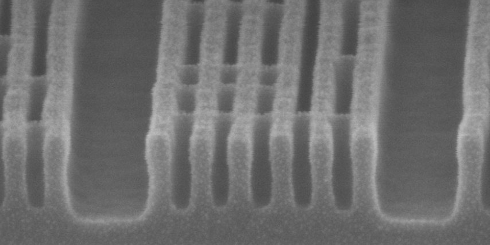
“In 2017, we already demonstrated that these 32nm pitch lines can be patterned directly with EUVL in one single exposure,” said Decoster. “Alternatively, a hybrid option can be used in which 193nm immersion lithography based self-aligned quadrupole patterning (SAQP) is combined with a direct EUV print of the block layer.” SAQP is a multi-patterning variant that relies on one lithography step (to create a pre-pattern of lines) and additional deposition and etch steps (to create spacer-like features). As a result, each initial line of the pre-pattern ends up in four lines with a four times denser pitch (Figure 1).

From EUVL single-patterning to EUVL multi-patterning
Meanwhile, it has become clear that EUVL single-patterning – and hence the advantages that it brings along – reaches its limits at 32nm to 30nm pitches. Decoster: “Beyond 30nm pitches, the use of current EUVL technologies (i.e., with 0.33 numerical aperture (NA)) will need to be complemented with multi-patterning techniques, which allow a further shrink of dimensions. These techniques in general involve splitting a chip pattern into two or more simpler masks and can exist in different flavors. Multi-patterning EUVL will be introduced somewhat sooner than originally thought – mainly due to the presence of stochastic failures.” These failures start to become more relevant at extremely small feature sizes and limit the practical resolution of single-exposure EUVL.
Multi-patterning options for the imec N5 technology node
In practice, this means that the most critical metal layers of the imec N5 (or foundry N3) technology nodes (with pitches as tight as 21nm) require EUVL multi-patterning techniques, such as self-aligned double patterning (SADP) or litho-etch litho-etch (involving two EUVL steps). Alternatively, imec showed that lines and trenches at these dimensions can still be achieved with 193nm immersion-based SAQP, or, alternatively, with immersion-based self-aligned octupole patterning (SAOP). Each of these techniques comes with its own set of advantages and disadvantages, in terms of cost-of-ownership, litho performance or complexity of the process flow.
“However, this is certainly not the end of EUVL single patterning,” clarifies Decoster. “We expect that the more relaxed metal layers (such as M4 to M7 layers) and the critical vias can still take advantage of EUVL single exposure for the following technology nodes (beyond imec N7 (foundry N5)). Also, imec and ASML are working on the next-generation of high-NA EUVL systems (with NA = 0.55), to further push the resolution for single exposures.”
Beyond imec N5: patterning options for 16nm pitch lines, trenches and blocks
Imec researchers have explored four different multi-patterning options for printing lines and blocks at pitches below 20nm: 193nm immersion based SAOP, EUV-based SADP, EUV-based SAQP, and self-aligned litho-etch litho-etch (SALELE). Decoster: “All four candidates have the potential of printing 16nm pitch lines. They differ however in terms of process complexity, cost-of-ownership, scalability and freedom in design – which are important considerations for the industry. We also found that line-edge roughness remains a major concern for the majority of the options.”
193nm immersion lithography can still do the job
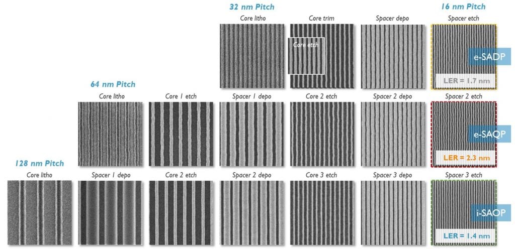
At these aggressive pitches, 193nm immersion lithography can only be used in combination with SAOP – which involves three times a patterning doubling approach, starting from 128nm pitches. Decoster: “The good thing about immersion-based SAOP is the small line-edge roughness. But an intrinsic drawback is the extremely long and complex process flow, which creates challenges for process control and cost.”
Shorter flows can be obtained with EUVL multi-patterning
“For this reason, we also explored ‘shorter’ EUVL-based multi-patterning flows, starting with EUV-based SADP”, adds Decoster. “To enable this double-patterning approach, the starting pitch at EUV lithography must be 32nm. Although current EUVL technology is still capable of printing 32nm pitch lines (which refers to the distance between the lines), the resulting line width can however not be printed smaller than 16nm. Therefore, we had to apply additional trimming techniques to realize the target 8nm lines at 32nm pitch. With the SADP technique, this pitch could successfully be reduced to 16nm.” 16nm pitch lines and trenches were also successfully printed with the more scalable EUVL SAQP approach – starting with an initial, more relaxed 64nm pitch. For these EUV-based multi-patterning approaches, line-edge roughness however remains an important issue. The team believes that this LER can be further reduced, e.g. by choosing the correct resist material and improving on resist smoothening (Figure 2).

eSALELE: a different approach to integrate blocks
All three multi-patterning approaches have one thing in common: first, the lines and trenches are printed, and later on, blocks are added – using e.g. a self-aligned block approach. The imec team also investigated a different approach using EUVL – called eSALELE – where lines and blocks are defined throughout the same process flow. Besides a relatively high LER, an additional drawback of this approach is the use of four EUV masks (two for the lines and two for the blocks) – making this concept more costly. Decoster: “But the main advantage of the eSALELE approach is the flexibility in design, and the avoidance of ‘dummy’ metal lines – printed lines that are not really needed for the chips operation. Avoiding these lines is beneficial for the RC delay and power consumption in the back-end-of-line.” The team is currently exploring the feasibility of printing 16nm pitch lines with the eSALELE technique.
Single exposure EUVL entering the memory field: the case of STT-MRAM
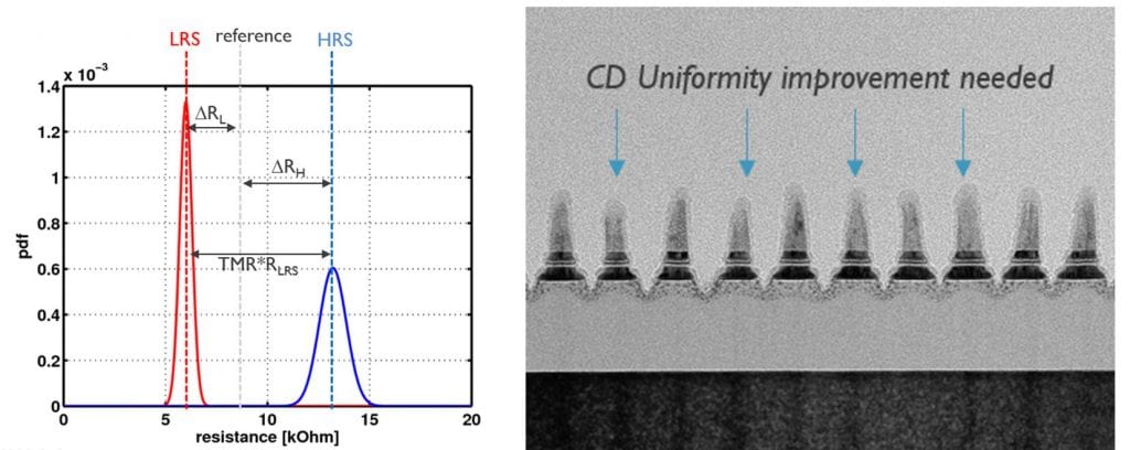
Due to its high writing and reading speed, STT-MRAM has recently emerged as a promising candidate for replacing SRAM-based last-level cache memories. The core element of an STT-MRAM device is a pillar-like magnetic tunnel junction, in which an insulating layer is sandwiched between two thin ferromagnetic layers which are the fixed and the free layers. The magnetic tunnel junction can exist in two different resistance states: a low resistance state (LRS, with the magnetization of the two magnetic layers in parallel) and a high resistance state (HRS, with the magnetization in an antiparallel state). Writing of the memory cell is performed by switching the magnetization for the free magnetic layer, by means of a current that is injected into the magnetic tunnel junction. The read operation relies on tunnel magnetoresistance (TMR), which is a function of the resistance difference between the two resistance states.
From immersion lithography to single exposure EUVL
So far, the pillars – i.e. the stacked layers forming the magnetic tunnel junction – have been patterned with 193nm immersion lithography to achieve 200nm, and, later on, 100nm pitch pillar pitches. Murat Pak, R&D engineer at imec: “But in order to meet the high-density requirement for future memories, we need tighter pitches such as 50nm or less – with pillar diameters of around 20nm (i.e., the pillar CD after full patterning). These aggressive pitches can no longer be achieved with immersion lithography, and this highlights the need for introducing single exposure EUVL.”
Introducing LCDU as the most critical metric
At these small dimensions, the impact of roughness and stochastic failures can however no longer be neglected – calling for improved patterning techniques. “For this memory application, the most critical parameter turns out to be the local CD uniformity (or LCDU), which is a measure for the pillar roughness,” explains Pak. “This LCDU will obviously impact the resistance variation, and hence the read performance of the STT-MRAM cell. Therefore, ensuring a good LCDU is critical in STT-MRAM manufacturing.”

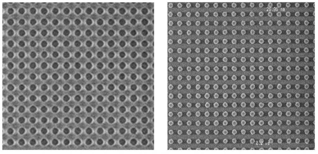
In order to optimize the LCDU of the magnetic tunnel junction pillars, different EUV litho processes have been proposed and compared. Pak: “First, we considered different resists, including the well-known chemically amplified resist (or CAR, which was initially optimized for 193nm immersion lithography), and two different MCR (or metal containing) resists. Second, our team screened different underlayers (including spin-on carbon and spin-on glass) – which is the layer underneath the resist – and studied their impact on the performance of the resist material. And finally, we studied different tonalities, in particular a negative tone CAR resist (creating pillars) and a positive tone resist in combination with a tone reversal process (‘turning’ holes into pillars),” (see Figure 4). The team also checked if the targeted improvements on the LCDU were transferred to the etch process. For all experiments, exposures have been performed using an ASML TWINSCAN NXE:3300B.

Three promising approaches
As a main conclusion, the two most promising approaches in terms of LCDU have been obtained with one type of MCR resist. A third option – making use of the tone reversal process – also performed well, mainly in terms of pillar LCDU as well. “For all three approaches, we obtained an improvement above 20% for the LCDU performance,” adds Murat Pak. “This is an important step towards the targeted LCDU of 1.55nm after full patterning.” For these promising litho process options, other performance metrics such as process window analysis, pillar circularity and critical dimension uniformity (i.e. CD uniformity within one or different wafers) have been verified as well.
Summary
In this article, various EUVL patterning approaches have been proposed for future logic and memory (i.e., SST-MRAM) applications. For logic, the performance of EUV-based SADP, EUV-based SAQP and EUV-based SALELE were compared with immersion-based SAOP. All options have the potential of printing metal line pitches and trenches as aggressive as 16nm. However, trade-offs have to be made in terms of process complexity, cost-of-ownership, freedom in design, and line-edge roughness. For SST-MRAM, three different EUV-based approaches have been identified for printing 50nm pitch magnetic tunnel junction pillars, with promising LCDU performance.
This is Part 1 in a two part series. Click here for Part 2, EUV Lithography: Sailing Along the Stochastic Cliffs.