
JIM O’NEILL, Chief Technology Officer, Entegris, Billerica, MA
The Fourth Industrial Revolution is surrounding us with technologies that did not exist a few years ago. Some of them were not even imagined a few decades earlier. Autonomous vehicles are already being tested on public streets. Drones are surveying landforms, shooting movies, and delivering packages. Vast amounts of video content, created by professionals and amateurs alike, are being shot and posted. Surveillance, both fixed and mobile, is becoming commonplace, server farms are bigger than ever, and 4G networks are being supplemented or replaced with 5G. What all these trends have in common is that they generate vast amounts of data that must be processed, transported, and stored faster and more reliably than ever before.
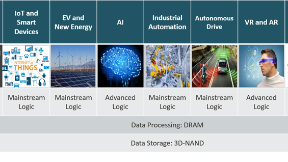
Many of these new applications will require advanced logic devices to achieve greater power and processing speeds to support them (Figure 1). Improvements in chip performance have already been achieved with smaller transistors, new design architectures, and higher-performance materials. However, continued device miniaturization below the 10 nm scale, the introduction of 3D architectures such as FinFET (Fin field effect transistors) and GAA (gate-all-around) transistors, and the use of new metals to reduce wiring delays and improve reliability have dramatically increased the complexity of chip manufacturing. In this environment, manufacturing yields are increasingly difficult to achieve, making the timely introduction of new logic devices more and more difficult. This paper looks at critical issues that will have to be addressed to cost-effectively produce these faster, denser chips.


The new lithography
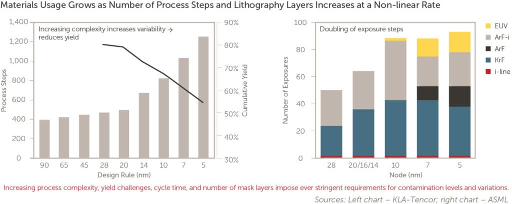
The continued shrinkage of logic devices brings new challenges to chip manufacturing. The ability to resolve fine patterns and place them accurately on the die is increasingly difficult at dimensions below 20 nm. Historically, the miniaturization process has been achieved through advances in optical lithography, a photographic process using optical masks to create patterns on a chip. The extent to which this miniaturization process can be extended is ultimately limited by the wavelength of the light that is used. Today’s 10 nm technology still uses light with a wavelength of 193 nm, so the size of the features on these devices is roughly 1/20th the wavelength of the light used to create them. This is a significant challenge requiring complex processing techniques (Figure 2). As features continue to shrink and today’s optical lithography pushes the physical limits imposed by the wavelength of the current ultraviolet light source, the technology has moved to even shorter wavelengths in the extreme ultraviolet (EUV) region of the spectrum. Along with its benefits, EUV lithography poses its own challenges in terms of the throughput of the optical scanner and control of defects on the optical mask.

Mask handling
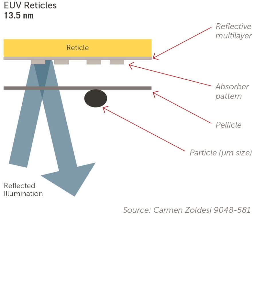
Traditional optical lithography operates by passing light through photomasks consisting of fused silica and a chrome metal-absorbing film. However, masks designed to work at shorter EUV wavelengths are fundamentally different in that they are reflective and require new materials for both their substrate and pattern film. These masks are extremely sensitive to defects within or on the multilayer stack. Pellicles are typically used to protect conventional optical masks from contamination, but the development of pellicles for EUV masks has been difficult and current pellicles cannot withstand high power EUV illumination (Figure 3). Cleaning EUV reticles once they have become contaminated is a significant challenge. The solution is designing specialized protective pods specifically for handling EUV reticles.

Physical and chemical challenges
In addition to lithography challenges, fine patterns themselves are sensitive to damage by small particles and subject to problems of structural integrity. Capillary effects can lead to pattern collapse during cleaning steps, and small defects and contaminants that could once be ignored can now ruin chips, either immediately or after they have been deployed. Depositing films over very small patterns with aspect ratios that can exceed 10:1 requires extremely conformal processes to achieve adequate coverage.
Materials
As chip dimensions shrink, wires that connect transistors on a chip require new metallurgies with lower resistivity to avoid signal delays and improve reliability. Copper has long been the preferred metal for interconnect wiring, but engineers have begun to explore materials with lower resistance such as cobalt, molybdenum, and ruthenium as replacement alternatives at the smallest wiring dimensions. Precursors for these materials and the processes used to deposit these films are still immature and will require further development before they are ready for high volume manufacturing. Increasing numbers of deposition precursors are solids and the challenge of deriving a gas from the solid state requires specialized handling and delivery equipment.
Dielectrics
As transistors become smaller, the gate insulator thickness must also shrink to enable sufficient current density through the channel. For decades, silicon dioxide (SiO2) was the go-to gate oxide material. But as gate dielectrics have decreased in size, they have become “leaky” at thicknesses less than 1.2 nm. Electron tunneling allows unacceptable levels of current leakage, which increases power consumption and reduces reliability. By using a material with a higher dielectric constant, the insulator thickness can be increased enough to prevent electrons from tunneling through it and yet permeable enough to let the gate’s electric field penetrate the channel to turn on the transistor. The solution to this challenge has been to replace silicon dioxide gate dielectrics with high-k materials like hafnium and zirconium-based oxides (HfO2 and ZrO2). These materials increase gate capacitance while controlling leakage.
Atomic Layer Processes
Small geometries with high aspect ratios (HAR) require extreme conformality if they are not to be damaged by deposition of subsequent layers. Atomic layer deposition (ALD) is an effective way to achieve this degree of conformality. The process deposits a few atomic layers of a material in each of multiple cycles. This allows high levels of control and enables nearly perfect film conformality. The processes can, in some cases, be engineered to allow the selective deposition of a film on one type of material but not another, enabling even greater process control. Similarly, the removal of thin films over small HAR structures often requires etch processes that can be controlled at atomic scale dimensions. These are called atomic layer etch (ALE) processes and like ALD allow fine degrees of control to lay down film layers without disturbing vulnerable underlying HAR features.
Killer contamination
Then there is contamination. As chip features shrink the potential impact of very small contaminants grows. Particles that would not have affected yesterday’s chips can become “chip killers” today. They can lower yield by causing immediate problems detectable by testing. But they can also lie dormant and cause failures in the field requiring costly replacement or recalls. In addition to these smaller particles, chipmakers must be concerned with dissolved ionic metal contaminants that can move through the gate oxide layer to form conduction channels and increase current leakage.
New materials must maintain near-perfect purity levels. Where contaminant levels at parts per billion or parts per trillion were once considered acceptable, semiconductor manufacturing will soon require purity levels measure in parts per quadrillion. And as chip densities increase, ever-smaller particles and metal impurities in resists or in process chemicals will produce yield-sapping flaws in the resulting chips. Contaminants that were once considered too small to affect the resulting chips can cause problems as features shrink, and older filtration technology may not effectively remove those ultra-small contaminants.
Significant advancements in filtration technology have combined porosity control in advanced polymer membranes with chemical activation of the membrane surface to selectively remove undesirable contaminants. But finer filtration alone is not the answer. As chemistry changes, there can be compatibility problems between the filters themselves and the chemicals used in chip production and cleaning. For example, complex cleaning formulations can be inadvertently “deactivated” if a critical component is removed through chemical interaction with the functionalized membrane.
Because chip production is a linear process, a defect or contaminant at any point in the process can affect the end product. The result can be either an immediate yield reduction or a latent defect that can lead to costly reliability failures in the field. Keeping the entire process clean with clean chemistry, compatible filter technology, and handling capability that maintains material integrity ensures maximum productivity. This will become more challenging yet more essential as chips get more complex and features shrink. Manufacturers who lead in addressing these new challenges will have significant advantages in the lucrative, high-end chip market.
Advanced filter technology
In simplistic terms, filters function as sieves, removing particles too large to fit through the filter’s mesh. Removing smaller particles requires a finer mesh. But today’s advanced filters, particularly those for the smallest particles, are significantly more complex. Polymer membranes are engineered as multilayer films or hollow fibers to maximize the flow of liquid while retaining the greatest amount of contaminant. Chemistry can be applied to functionalize the surface of the membrane to activate the removal of specific contaminants through an absorptive process. The challenge is that unlike a sieving filter, which can be chemically inert, a chemically active surface must be compatible with all the components of a complex formulation.
Effective wafer handling
The word “travel” comes from “travail,” which suggests hardship and stress. That is as true for wafers in a fab as for the traveler passing through a modern airport, and smaller, more compact chips are increasingly susceptible to damage in handling or transit. As a wafer moves through the process sequence, it becomes more valuable, so protecting the wafer becomes even more important as it progresses through the build cycle.
Wafers spend most of their time in the fab within minienvironments called front-opening unified pods (FOUPs). While FOUPs are designed to protect the wafer from the effects of external contamination, a significant challenge comes from the wafers themselves. When wafers return to a FOUP after a given process step, they can outgas material from the chemistry to which they were exposed thereby contaminating the FOUP. The resulting contamination can affect films exposed in subsequent process steps. The longer wafers reside in a FOUP, the greater the chance of contamination from outgassing. Fab operations often place limits on the amount of time a wafer can reside in a FOUP before subsequent processing for particularly sensitive steps. Such time constraints reduce the flexibility and productivity of the fab. To prevent such problems, FOUP construction materials have been engineered to minimize the effect of outgassing. Gettering and purge capabilities have been added as well. Minimizing the environmental contamination is a key feature of an effective FOUP.
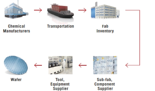
The material supply chain within the semiconductor industry is extremely complex. The path that materials follow from the point where they are manufactured to the point where they are used on the wafer may take several months and span several continents (Figure 4). There are plenty of opportunities to contaminate a material as it makes its way along this path. It is no longer sufficient for a material supplier to simply manufacture a pure material. The integrity of that material must be maintained from the point of manufacture to the point of use.

Because of the increasing challenge that semiconductor manufacturers face in achieving the process yields necessary to meet timely introduction cycles of denser chips, every aspect of the fabrication process must be controlled to exacting standards as wafers move through the fab. In addition to their own processes, chip manufacturers must be concerned with controlling processes further back along the supply chain to ensure that the materials and chemicals they use are clean and reliable. Without such controls all along the supply chain, achieving adequate manufacturing yield is difficult.
The second reason to be concerned with the material supply chain is the increasing complexity of the manufacturing process and the compatibility of materials that are used. While new materials can bring significant benefits to device or process performance, an understanding of the interactions of these materials with each other or with components in the process is essential. Gases released within a FOUP in one chemical process can affect the next and must be purged to avoid contamination. New, advanced filters with chemically active surfaces must be paired with appropriate chemicals to avoid damaging interactions. When new materials and equipment are individually sourced, responsibility for avoiding problems falls on the chipmaker’s process engineers. Working with suppliers that address multiple aspects of the process adds their engineers and experience to your team and reduces the risk of problematic interactions. This is particularly true when adopting new processes.
Summary
New technologies and processes will enable efficient production of denser, faster, more powerful chips. Taking advantage of those technologies will require flexibility, care, and attention to detail, but the payoff will be leadership in the most profitable segment of a growing market. As features continue to shrink, the physics will demand new materials for smaller transistors, thinner dielectrics, and interconnect wiring. The features themselves, being both smaller and having higher aspect ratios, will be more vulnerable to damage in manufacturing and handling, requiring new processes and tools.
The lithographic processes used to produce tomorrow’s smaller features are changing, not just in size, but in type. These new processes will affect the chemistry and handling of reticles for extreme ultraviolet lithography and the masks themselves. Deposition precursors and plating formulations will change along with delivery systems for the new materials. Every aspect of production will be affected by the need to eliminate smaller particles and toxic gases and reduce the concentration of metallic ions, and equipment like filters, tanks, and piping will have to be compatible with chemicals to prevent in-process contamination.
Chipmaking is a “cascading” process. Each of the inputs—materials or process—flows directly into the finished chips, interacting with other materials and processes along the way. When gearing up to produce advanced logic chips, it is critical to consider the integrity of each of those inputs along with their interactions to ensure a positive impact on efficiency, yield, and profit.
New technologies and processes will enable efficient production of denser, faster, more powerful chips. Taking advantage of those technologies will require flexibility, care, and attention to detail, but the payoff will be leadership in the most profitable segment of a growing market.
Lithographic processes are changing to enable production of finer detail. The shorter wavelength of EUV light will enable printing of those smaller features, but the masks themselves will be vulnerable to damage or contamination in new ways and will require different technology for cleaning and handling.
Finer patterns will require new materials, both those that chips are made of and those used in their production. Copper for interconnect wiring experiences greater resistance at very small dimensions and will be increasingly replaced with metals with lower resistance including cobalt, ruthenium, and molybdenum. SiO2 has been replaced as a dielectric with high-k materials such as oxides of hafnium and zirconium to increase gate capacitance while preventing leakage due to electron tunneling. Plating formulations for high aspect ratio (HAR) will have to change to enable seamless fill of small structures from the bottom up.
Many deposition precursors, particularly those for metal and metal oxide films, are solids and will require specialized handling and delivery equipment. Complicated film stacks require increasingly clean, complex chemical formulations to enable extreme selectivity among materials in the stack.
High aspect ratio (HAR) features will be particularly vulnerable during production. They will require specialized plating formulations and appropriate deposition precursors to prevent damage in the course of ALD processes. Clean formulations will be increasingly important as patterning and metal stacks grow more complex.
Smaller features and more complex architectures will be susceptible to smaller particles and lower concentrations of metal ions. The materials from which chips are built will have to be cleaner as will the chemical used in processing. Advanced filters will remove particles by chemical adhesion as well as physical sieving and will have to be chemically compatible with the formulations they handle. Contamination control will be expected of both chemical suppliers and at every step of the manufacturing process.
Throughout the fab, wafers and reticles will have to be carefully handled to avoid damage or contamination. The same is true of liquid cleaning formulations and deposition precursors and for safe handling of toxic gases both before and after their use.
Chipmaking is a “cascading” process. Each of the inputs—of materials or processes—flows directly into the finished product, interacting with other materials and processes along the way. It is critical to consider the integrity of each of those inputs, along with their interactions, in gearing up to produce advanced logic chips. Vendors’ engineers can be a valuable resource in developing, updating, and maintaining a production system and can have a significant impact on a fab’s products, efficiency, yield, and profit.