By SRI SAMAVEDAM, senior vice president of CMOS technologies at imec, Leuven, Belgium
In the past few decades, growth of the global semiconductor industry has been driven largely by the demand for cutting-edge electronic devices such as desktops, laptops and wireless communication products, and by the rise of cloud-based computing. Growth will continue with new application drivers for the high-performance compute market segment.
First, the amount of data keeps on growing exponentially, a trend that will be accelerated by the rollout of 5G networks. We need more and more servers where these data are processed and stored. Following a 2020 Yole report [1], a compound annual growth rate of 29% is expected for the high-end central processing units (CPUs) and graphical processing units (GPUs) that are at the heart of these servers. They will support a host of datacenter applications, such as supercomputing and high-performance-computing as a service. Faster growth rate is expected for GPUs – triggered by emerging applications such as cloud gaming and artificial intelligence. Recent corona-related remote work and education will also leave their mark on the internet traffic. In March 2020, for example, internet traffic increased by nearly 50% and commercial internet data exchange in Frankfurt set a new world record [2] for data throughput at more than 9.1 Terabits per second.
A second main driver is mobile systems-on-chips (SoCs) – the chips in our smart phones. This market segment is not growing as fast, but the demand for more functionality in these SoCs in form-factor constrained chip area will drive further technology innovations.
Beyond the traditional dimensional scaling of logic, memory and 3D interconnects, these emerging applications will need to leverage cross-domain innovations. There is a need for new modules, new materials and architecture changes at the device, block and SoC level to realize the benefit at a system level. Below, these innovations are summarized in five major semiconductor technology trends.
Trend 1: Moore’s Law will continue for the next 8 to 10 years…
CMOS transistor density scaling will roughly continue to follow Moore’s Law for the next eight to ten years. This will be enabled mainly by advances in EUV patterning and by the introduction of novel device architectures which will enable logic standard cell scaling.
Extreme ultraviolet (EUV) lithography was introduced in the 7nm technology node to pattern some of the most critical chip structures in one single exposure step. Beyond the 5nm technology node (i.e., when critical back-end-of-line (BEOL) metal pitches are below 28-30nm), multi-patterning EUV lithography becomes inevitable – adding significantly to the wafer cost. Eventually, we expect high-numerical-aperture (high-NA) EUV lithography to become available for patterning the most critical layers of the industry’s 1nm node. This technique will push the multi-patterning of some of these layers back to single patterning, providing cost, yield and cycle-time relief (FIGURE 1).

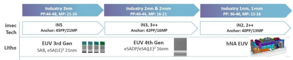
Imec contributes to advancing EUV lithography for example by investigating stochastic defectivity. Stochastic printing failures are random, non-repeating, isolated defects such as microbridges, locally broken lines and missing or merged contacts. Improvement in stochastic defectivity could lead to the use of lower dose exposures and thus improve throughput and cost. We try to understand, detect and mitigate stochastic failures and could recently report an order of magnitude improvement in stochastic defectivity.
To accelerate the introduction of high-NA EUV, we are installing Attolab – allowing to test some of the critical materials for high-NA EUV (such as mask absorber layers and resists) before the high-NA tool will be available. The spectroscopic characterization tools in this lab will allow us to look at crucial EUV-photon reactions with resists at attosecond timeframes, which are also relevant to understand and mitigate stochastic defect formation. Today, we have successfully completed phase one of the Attolab installation and expect to have high-NA EUV exposures in the coming months.
Apart from advancements in EUV lithography, Moore’s Law cannot continue without innovations in the front-end-of-line (FEOL) device architecture (FIGURE 2). Today, FinFET devices are the mainstream transistor architectures, with the most advanced nodes having 2 fins in a 6-track (6T) standard cell. However, scaling down FinFETs to 5T standard cells results in fin depopulation with only 1 fin per device in the standard cell, causing a dramatic drop in the device performance per unit area. Vertically stacked nanosheet devices are considered as the next generation device, being a more efficient use of the device footprint. Another critical scaling booster is the buried power rail (BPR). Buried in the chip’s FEOL instead of in the BEOL, these BPRs will free up interconnect resources for routing.

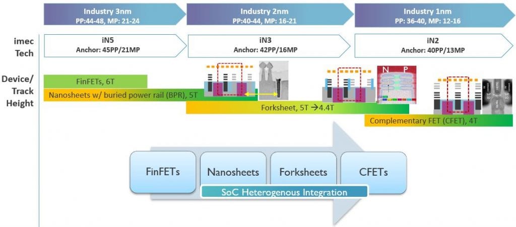
Scaling nanosheets into the 2nm generation will be limited by n-to-p space constraint. Imec envisions the forksheet architecture as the next generation device. By defining the n-to-p space with a dielectric wall, the track height can be further scaled. Another standard cell architecture evolution that will help with routing efficiency is a vertical-horizontal-vertical (VHV) design for metal lines, as opposed to traditional HVH designs. Ultimate standard cell scaling down to 4T will be enabled by complementary FETs (CFETs), that fully exploit the third dimension at the cell level by folding n-FETs over p-FETs or vice-versa.
Trend 2: … but logic performance improvement at fixed power will slow down
With the above-mentioned innovations, we expect transistor density to follow the path mapped out by Gordon Moore. But node-to-node performance improvements at fixed power – referred to as Dennard scaling – have slowed down due to the inability to scale supply voltage. Researchers worldwide are looking for ways to compensate for this slow-down and further improve the chip’s performance. The aforementioned buried power rails are expected to offer a performance boost at system level due to improved power distribution. Besides, imec looks at incorporating stress into nanosheet and forksheet devices, and at improving the contact resistance in the middle-of-line (MOL). Further out, the sequential CFET device will provide the flexibility for incorporating high mobility materials since the n-device and p-device can be optimized independently.
2D materials such as tungsten disulfide (WS2) in the channel promise performance improvements because they enable more aggressive gate length scaling than Si or SiGe. A promising 2D-based device architecture involves multiple stacked sheets each surrounded by a gate stack and contacted from the side. Simulations suggest these devices can out-perform nanosheets at scaled dimensions targeting 1nm node or beyond. At imec, dual-gate transistors with bilayer WS2 on 300mm wafers have already been demonstrated, with gate lengths down to 17nm. To further improve the drive current of these devices, we strongly focus on improving the channel growth quality, incorporating dopants and improving contact resistance in these novel materials. We try to speed up the learning cycles for these devices by correlating physical properties (such as growth quality) with electrical properties.
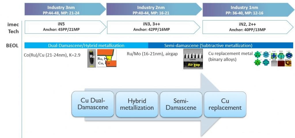
Besides the FEOL, routing congestion and RC delay in the BEOL have become important bottlenecks for performance improvement (FIGURE 3). To improve the via resistance, we are looking at hybrid metallization using Ru or Mo. We expect semi-damascene metallization modules to simultaneously improve resistance and capacitance in the tightest pitch metal layers. Semi-damascene will allow us to increase the aspect ratio of the metal lines (to lower resistance) by direct patterning and use airgaps as a dielectric in between the lines (to control the capacitance increase). At the same time, we screen a variety of alternative conductors like binary alloys as a replacement for ‘good old’ Cu, to further reduce the line resistance.

Trend 3: More heterogeneous integration, enabled by 3D technologies
In industry, we see more and more examples of systems being built through heterogeneous integration leveraging 2.5D or 3D connectivity. These options help address the memory wall, add functionality in form-factor constrained systems or improve yields on large chip systems. With the slowing logic PPAC (performance-power-area-cost), smart functional partitioning of SoC (system on chip) can provide another knob for scaling. A typical example is high-bandwidth memory (HBM) stacks, consisting of stacked dynamic random access memory (DRAM) chips that connect directly through a short interposer link to processor chip, such as a GPU or CPU. More recent examples include die-on-die stacking in Intel’s Lakefield CPU or chiplets on interposer in case of AMD’s 7nm Epyc CPU. In the future, we expect to see many more of these heterogeneous SoCs – as an attractive way to improve system performance.
At imec, we bring about the benefits at SoC level by leveraging innovations that we are making across the different domains (such as logic, memory, 3D…). In order to connect the technology options to the performance at system level, we have set up a framework called S-EAT (System benchmarking for Enablement of Advanced Technologies). This framework allows us to evaluate the impact of specific technology choices on the system level performance. For example: can we benefit from 3D-partitioning the on-chip memory at lower levels of the cache hierarchy? And what happens at the system level if static random access memory (SRAM) is replaced by a magnetic RAM (MRAM) memory?
As an illustration, we have used this platform to find the most optimal partitioning of a high performance mobile SoC containing a CPU and L1, L2 and L3 caches. In a traditional design, the CPU would reside next to the caches in a planar configuration. We assessed the impact of moving the caches to another chip, stacked with 3D wafer bonding techniques to the CPU chip. As the signals between cache and CPU now travel shorter distances, an improvement in speed and latency can be expected. The simulation experiments concluded that it was most optimal to move L2 and L3 caches to the top tier instead of L1 only or all 3 caches simultaneously.
To enable partitioning at these deeper levels of the cache hierarchy, a high-density wafer-to-wafer stacking technology is required. We have demonstrated wafer-to-wafer hybrid bonding at 700nm interconnect pitch and believe the advancements in bonding technology will enable 500nm pitch interconnects in the near future.
Heterogeneous integration is enabled by 3D integration technologies such as die-to-die or die-to-Si-interposer stacking using Sn microbumps or die-to-silicon using hybrid Cu bonding. The state-of-the-art Sn microbump pitches in production have saturated at about 30µm. At imec, we are pushing the boundaries of what is possible today. We have demonstrated a Sn-based microbump interconnect approach with interconnect pitch down to 7µm. Such high-density connections leverage the full potential of through-Si via technology and enable >16x higher 3D interconnect densities between die or between dies and a Si-interposer. This allows for a strongly reduced SoC area requirement for the HBM I/O interface (from 6 down to 1 mm2) and potentially shortens the interconnect lengths to the HBM memory stack by up to 1 mm. Direct bonding of die to silicon is also possible using hybrid Cu bonding. We are developing die-to-wafer hybrid bonding down to 3µm pitches with high tolerance pick and place accuracy, leveraging the learning from wafer to wafer hybrid bonding.
As SoCs are becoming increasingly more heterogeneous, the different functions on a chip (logic, memory, I/O interfaces, analog, …) need not come from a single CMOS technology. It may be more advantageous to use different process technologies for different sub-systems to optimize design costs and yield. This evolution can also answer the needs for more chip diversification and customization.
Trend 4: NAND and DRAM being pushed to their limits; emerging non-volatile memories on the rise
The total memory IC market forecast [3] suggests that 2020 will be a flat year for memory relative to 2019 – an evolution that can partly be related to the COVID-19 slowdown. Beyond 2021, this market is expected to start growing again. The emerging non-volatile memory market [4] is expected to grow at >50% compound annual growth rate – mainly driven by the demand for embedded magnetic random access memory (MRAM) and standalone phase change memory (PCM).
NAND storage will continue to scale incrementally, without disruptive architectural changes in the next few years. Today’s most advanced NAND products feature 128 layers of storage capability. The 3D scaling will continue with additional layers potentially enabled by wafer-to-wafer bonding. Imec contributes to this roadmap by developing low resistance word-line metals like ruthenium, researching alternate memory dielectric stacks, improving channel current and identifying ways to control the stress that evolves due to the growing number of stacked layers. We also focus on replacing the planar logic transistors in the NAND periphery with more advanced FinFET devices. We are exploring 3D ferroelectric FETs (FeFETs) with novel wurtzite materials as 3D NAND replacement in high-end storage applications. As a replacement for traditional 3D NAND, we are evaluating the feasibility of novel types of memories.
For DRAM, cell scaling is slowing down, and EUV lithography may be needed to improve patterning. Samsung recently announced EUV DRAM production for their 10nm (1a) class. Besides exploring EUV lithography for patterning critical DRAM structures, imec provides the building blocks for true 3D DRAM solutions. And this starts with putting the memory array on top of the periphery. Such an architecture requires a low thermal budget deposited semiconductor for the array transistors. And this is where low temperature IGZO (or indium-gallium-zinc-oxide) family of transistors enter the scene. We have demonstrated 40nm gate length IGZO devices with Ion/Ioff ratio >1E12. And we continue to explore alternate low temperature semiconductors using ab-initio simulations and experiments to meet the stability, mobility and reliability requirements. Ultimate 3D DRAM implementation will also require these materials to be deposited on topography. This drives the need for atomic layer deposition (ALD) for the layer formation. Finally, just as with NAND, we look at enabling a FinFET-based periphery with high-k/metal gate structures as a replacement for planar transistors with poly-Si gates.
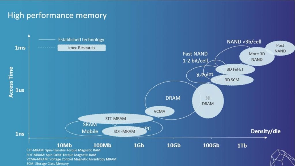
In the embedded memory landscape, there are significant efforts to understand – and eventually tear down – the so-called memory wall: how quickly can the CPU access data from DRAM or from SRAM-based caches? How do you ensure cache coherency with multiple CPU cores accessing a shared cache? What are the bottlenecks that limit speed, and how can we improve the bandwidth and data protocols that are used to fetch the data? Imec deploys its system-level simulator platform S-EAT to gain insights into these bottlenecks. This framework also allows for evaluation of novel memories as SRAM replacements to understand the system performance for various workloads. We are studying various kinds of magnetic random access memories (MRAM) including spin-transfer torque (STT)-MRAM, spin-orbit torque (SOT)-MRAM and voltage controlled magnetic anisotropy (VCMA)-MRAM) to potentially replace some of the traditional L1, L2 and L3 SRAM-based caches (FIGURE 4). Each of these MRAM memories comes with its own benefits and challenges and may help us overcome the memory bottleneck by improving speed, power consumption and/or memory density. To further improve density we are also actively researching selector devices that can be integrated with the magnetic tunnel junctions – which are at the heart of these MRAM devices.

Trend 5: Spectacular rise of the edge AI chip industry
With an expected growth of above 100% in the next five years, edge AI is one of the biggest trends in the chip industry. As opposed to cloud-based AI, inference functions are embedded locally on the Internet of Things (IoT) endpoints that reside at the edge of the network, such as cell phones and smart speakers. The IoT devices communicate wirelessly with an edge server that is located relatively close. This server decides what data will be sent to the cloud server (typically, data needed for less time-sensitive tasks, such as re-training) and what data gets processed on the edge server.
Compared to cloud-based AI, in which data needs to move back and forth from the endpoints to the cloud server, edge AI addresses privacy concerns more easily (FIGURE 5). It also offers advantages of response speeds and reduced cloud server workloads. Just imagine an autonomous car that needs to make decisions based on AI. As decisions need to be made very quickly, the system cannot wait for data to travel to the server and back. Due to the power constraints typically imposed by battery-powered IoT devices, the inference engines in these IoT devices also need to be very energy efficient.


Today, commercially available edge AI chips – the chips inside the edge servers – offer efficiencies in the order of 1-100 tera operations per second per Watt (Tops/W), using fast GPUs or ASICs for computation. For IoT implementations, much higher efficiencies will be needed. Imec’s goal is to demonstrate efficiencies for inference in the order of 10.000 Tops/W.
We are pursuing a different approach by looking at analog compute-in-memory architectures. This approach breaks with the traditional Von Neumann computing paradigm, that is based on sending data from memory to a CPU (or GPU) for computations. With analog compute-in-memory, computation is done inside a memory framework, saving a lot of power in moving data back and forth. In 2019, we demonstrated an SRAM-based analog compute-in-memory cell (built in 22nm FD-SOI technology) achieving 1000Tops/W efficiency. To further improve this number towards 10.000Tops/W, we are researching non-volatile memories such as SOT-MRAM, FeFET and IGZO-based memories.
About the author


Sri Samavedam is senior vice president of CMOS technologies at imec since August 2019. His responsibilities include programs in logic, memory, photonics and 3D integration. Prior to that, he was senior director of technology development at GlobalFoundries in Malta, NY, where he led qualification of 14nm FinFET technology and derivatives into volume production and early development of 7nm CMOS. He began his research career at Motorola in Austin, TX, working on strained silicon, metal gates, high k dielectrics and fully-depleted SOI devices. He holds a Ph.D. in Materials Science and Engineering from MIT and a masters from Purdue University.
References
1. High-end CPU and GPU: HPC and cloud gaming are setting the bar for leadership http://www.yole.fr/xPU_HighEnd_CPU_GPU.aspx
2. DE-CIX sets a new world record: More than 9 Terabits per second data throughput at Frankfurt Internet Exchange https://www.de-cix.net/
3. Memory Market Not Forecast to Exceed 2018 High of $163.3B until 2022. IC Insights, April 28, 2020. https://www.icinsights.com/
4. After the 3D XPoint take-off, emerging NVM keeps growing. http://www.yole.fr/ENVM_IndustryUpdate.aspx
5. A view on the memory landscape and how imec contributes.