Hamish Rossell, Product Applications Manager, Scientific Solutions Group, Olympus, Waltham, MA


Microscopy has always played a pivotal role in the semiconductor industry as inspectors need to quickly and efficiently identify and image defects on wafers in a repeatable way. Until recently, the wide range of contrast techniques and magnifications needed to complete these inspections made the process difficult.
With optical microscopes, semiconductor inspections required multiple systems, skilled operators, and complex work instructions to achieve the necessary results—taking up valuable space and resources. But with modern systems inspections are faster and more repeatable than ever before.
In this article, we will explore how the powerful macro-to-micro viewing capabilities of digital microscopes overcome common challenges in the inspection process.
The challenges of using conventional microscopes for semiconductor inspections
A conventional compound microscopy inspection relies on switching from one fixed magnification to another, and the lowest magnification has a field of view around 8 mm. To see more of your sample, you would need to manually stitch the image, significantly modify the microscope, or move the sample to a stereo microscope.
In contrast, the largest field of view available on the most recent DSX series digital microscope is 19.2 mm. This is usually enough to capture an entire overview in one image. Keep reading to learn more about the macro observation benefits of digital microscopes.
Macro
The capabilities of digital microscopes extend beyond a wide magnification range. Adding motorized components to the microscope extends the system’s functionality even further.
For larger samples that extend beyond your system’s field of view, you can quickly and easily capture images of the entire sample using the automated stitching function and a motorized X, Y, Z stage on a low-power objective.
The result is a fully focused, high-resolution image you can use to show larger features of interest or provide context for further analysis. With a maximum stage travel range of 300 mm × 300 mm, entire wafers can be imaged quickly to provide an overview map.
This map will both show macro scale defects and serve as a navigation aid as the operator increases magnification. It may be useful to initially image at this low magnification level using different observation techniques to highlight contamination.
With the ability to work and image with different techniques at the press of a button, you can save significant time in your inspection workflow.
Micro
Typically, the next step following macro observation is to change systems or disassemble and reassemble some other digital microscopes. This causes a loss of position and focal point.
Using the Olympus DSX1000 digital microscope, you can exchange the objective lens without the risk of exposing the camera to contamination or the sample to unnecessary movement, all while maintaining position data and focus. The captured macro map can now be used to quickly navigate the sample and provide a view of multiple image acquisition areas.
With the addition of zoom optics, you can use the full optical range of each objective. To quickly magnify a feature of interest, there is no need to change the objective or rely on digital zoom. The DSX zoom optics will bridge multiple conventional objective magnifications, reducing the need for an objective change, parts to store, and movement over the sample.
It is nearly impossible to present a perfectly planar sample perpendicular to the viewing plane—something that has caused issues for microscopists for decades. The conventional methods to do this were either significantly compromised, such as using an inverted microscope system, or used complex and space-consuming vacuum and levelling systems.
This is not the case in modern digital microscopy, where developments in 3D acquisition and autofocus have made it possible to acquire and analyze even the roughest or most uneven samples using a wide range of techniques.
On the DSX1000 digital microscope, a field of view of as little as 55 μm is achievable with submicron resolution. This can be done using an Olympus UIS2 objective with planar and apochromatic correction and a 0.95 numerical aperture (NA). In other words, an objective built to provide a perfectly flat, undistorted image with color correction beyond the visible spectrum and the highest level of detail and resolution from an air objective.
Advanced analysis
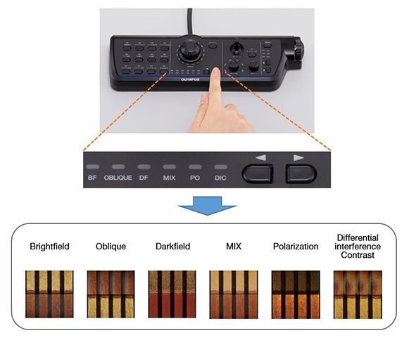
As mentioned earlier, a big plus of modern digital systems is that they can take the guesswork out of imaging by combining repeatability with ease of use. In the DSX1000 digital microscope, multiple observation techniques (brightfield, oblique, darkfield, MIX, polarized light, and true differential interference contrast) are available at the touch of a button. As a result, finding the correct technique is a straightforward process, especially when using the desktop controller to increase ergonomics and efficiency.
To choose your observation method, you can either sequentially select it or find the optimal one using the Best Image function (FIGURE 1). With this function, the system automatically images the sample under preset conditions and displays thumbnail images of your sample under the different methods. This makes it quick and easy to choose the right one, since you can simultaneously view them and choose the method that best shows the features or defects.

Now let’s put these observation methods into practice by exploring a typical use case.
Example of a typical use case
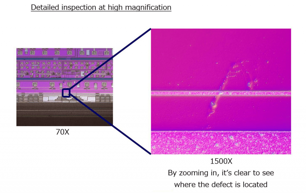
FIGURE 2 is an image of a semiconductor wafer with a defect. This defect is hard to see under some conditions, so finding the correct observation method can be time-consuming on a conventional system.

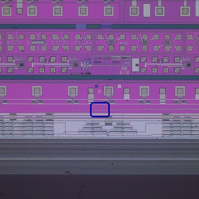
By selecting darkfield, you can see that the defect is slightly more visible, as shown in FIGURE 3.
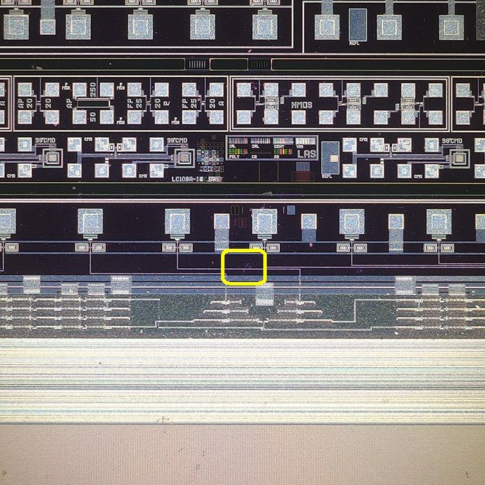
Certainly, the defect is more visible—but what about using DIC? With the push of a button, the microscope will insert the polarizer, analyzer, and motorized and encoded DIC prism needed for this observation method (FIGURE 4).
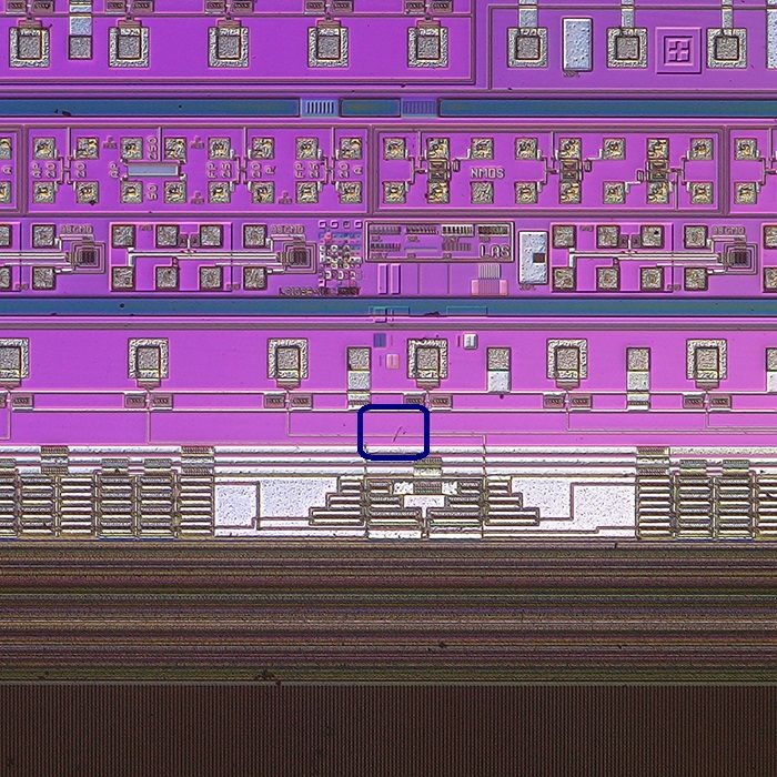
In DIC observation, the defect is now highly visible, and the conditions required to achieve this are recorded in the image. These conditions can be saved with the image and as an option for the operator to use in the future (FIGURE 5).

Guaranteed accuracy and precision
In semiconductor inspections, the integrity of data and measurements is critical. Without a guaranteed measurement, the microscope is simply a subjective observation tool. The DSX1000 digital microscope has integral calibration tools that, when performed by an Olympus certified technician, will calibrate every objective at every magnification to a traceable standard.
While the focus of this piece has been on semiconductor inspection, the versatility of the digital microscope is limitless. From macro inspection of test pads, to micro inspection of contamination, to optional fluorescence observation, digital microscopes are assets to any inspection environment.