Last month in Nature Communications (doi:10.1038/ncomms5836) IBM researchers Jeehwan Kim, et al. published “Principle of direct van der Waals epitaxy of single-crystalline films on epitaxial graphene.” They show the ability to grow sheets of graphene on the surface of 100mm-diameter SiC wafers, the further abilitity to grow epitaxial single-crystalline films such as 2.5-μm-thick GaN on the graphene, the even greater ability to then transfer the grown GaN film to any arbitrary substrate, and the complete proof-of-manufacturing-concept of using this to make blue LEDs.
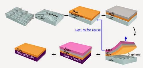
The figure above shows the basic process flow. The graphenized-SiC wafer can be re-used to grow additional transferrable epi layers. This could certainly lead to competition for the Leti/Soitec/ST “SmartCut” approach to layer-transfer using hydrogen implants into epi layers.
No mention is made of the kinetics of growing 100mm-diameter sheets of single-crystalline GaN on graphene. Supplemental information in the online article mentions 1 hour at 1250°C to cover the full wafer, but the thickness grown in that time is not mentioned. From first principles of materials engineering, they must either:
A) Go slow at first to avoid independent islands growing to form a multicrystalline layer, or
B) Initially grow a multicrystalline layer and then zone anneal (perhaps using a scanned laser) to transform it into a single-crystal.
In either case, we would expect that after just a few single-crystalline atomic layers had been either slowly grown or annealed, that a 2nd much-higher speed epi process would be used to grow the remain microns of material. More details can be seen in the EETimes write up.
—E.K.