The IEEE 2022 Symposium on VLSI Technology and Circuits attracted 650 people to attend in person in Honolulu, and an equal number of virtual attendees.
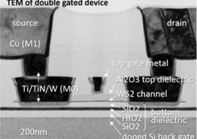
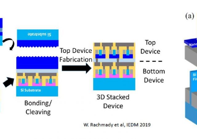
A 300mm Platform for 2D-Material Based MOSFET Devices
2D materials, a family of materials that form two-dimensional crystals, promise to enable a broad range of semiconductor applications, such as selectors or back-end compatible transistors.
Photoelectric measure of atomically thin stacks
A team led by researchers at the University of Warwick have discovered a breakthrough in how to measure the electronic structures of stacked 2D semiconductors using the photoelectric (PE) effect. Materials scientists around the world have been investigating various heterostructures…
Controlling Polymers to Tune TFTs
Thin-film transistors (TFT) created using only additive process steps could create new low-cost ICs with functionalities beyond silicon, but only if we understand how to control structures at the molecular level. Thin films of conjugated polymers such as poly(3-hexylthiophene) (P3HT)…
Micro-Buckled 3D Silicon Scaffolds
A new silicon microstructural solution announced this month is so powerful in creating 3D patterns from 2D surface machining that I just have to share. The figure shows 3D silicon microstructures formed by compressive buckling. The method can be used…
NanoParticle Self-Assembly at UofM
Theory and Practice synergize R&D Sharon C. Glotzer and Nicholas A. Kotov are both researchers at the University of Michigan who were just awarded a MRS Medal at the Materials Research Society (MRS) Fall Meeting in San Francisco for their…
IBM Shows Graphene as Epi Template
Last month in Nature Communications (doi:10.1038/ncomms5836) IBM researchers Jeehwan Kim, et al. published “Principle of direct van der Waals epitaxy of single-crystalline films on epitaxial graphene.” They show the ability to grow sheets of graphene on the surface of 100mm-diameter…
Moore’s Law is Dead – (Part 4) Why?
We forgot Moore merely meant that IC performance would always improve (Part 4 of 4) IC marketing must convince customers to design ICs into electronic products. In 1965, when Gordon Moore first told the world that IC component counts would…
Moore’s Law is Dead – (Part 3) Where?
…we reach the atomic limits of device scaling. At ~4nm pitch we run out of room “at the bottom,” after patterning costs explode at 45nm pitch. Lead bongo player of physics Richard Feynman famously said, “There’s plenty of room at…
Moore’s Law is Dead – (Part 2) When?
…economics of lithography slow scaling. Moore’s Law had been on life support ever since the industry started needing Double-Patterning (DP) at 1/4-pitch of 193nm optical lithography. EUV lithography shows slow and steady progress in source and resist technologies, and ASML…