By Dr. Yu-Han Chang, Senior Technology Analyst at IDTechEx
Why Is Advanced Semiconductor Packaging Needed?
This is a data-centric world. The growing amount of data generated in various industries increasingly drives the demand for high-bandwidth computing. Applications such as machine learning and AI require powerful processing capabilities, leading to the need for dense transistor placement on chips and compact interconnection bump pitches in packaging. The latter highlights the significance of semiconductor technologies in meeting these requirements.
Semiconductor packaging has evolved from board-level to wafer-level integration, bringing notable advancements. Wafer level integration provides advantages over traditional methods, such as increased connection density, smaller footprints for size-sensitive applications, and enhanced performance.
“Advanced” semiconductor packaging specifically includes high-density fan-out, 2.5D, and 3D packaging, characterized by a bumping pitch size below 100 µm, enabling at least 10x higher interconnect densities.
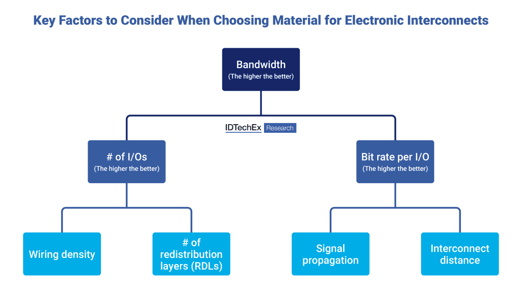
Bandwidth Is Key
To enhance bandwidth from a packaging perspective, two key factors come into play: the total number of I/Os (input/output) and the bit rate per each I/O. Increasing the total number of I/Os requires enabling finer line/space (L/S) patterns in each routing layer/redistribution layer (RDL) and having a higher number of routing layers. On the other hand, improving the bit rate per I/O is influenced by the interconnect distance between chiplets and the selection of dielectric materials. These factors directly impact the overall performance and efficiency of the packaging system.

Unleashing High Bandwidth: Exploring Materials and Processing for Advanced Semiconductor Packaging
Delving deeper into achieving higher wiring density and a higher bit rate per I/O from a materials and processing perspective reveals the critical role played by the selection of dielectric materials and the utilization of appropriate processing techniques. These factors have a significant impact on the overall performance and capabilities of the packaging system.

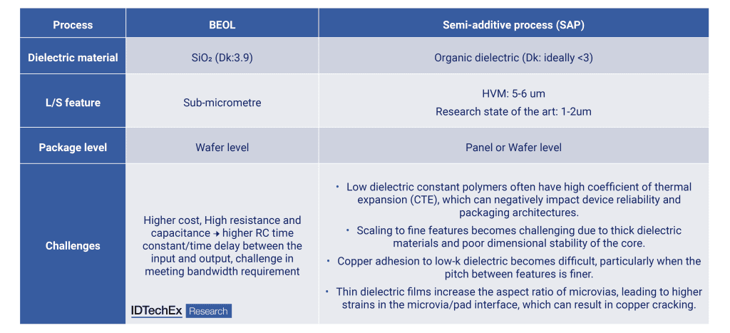
Selecting suitable dielectric materials is crucial, considering properties like low dielectric constant, optimal CTE (as close to the CTE of Cu as possible), and favorable mechanical characteristics that ensure module reliability, such as Young’s modulus and elongation. These choices enable higher data rates while preserving signal integrity and facilitating fine line/space features for increased wiring density.
In high-performance accelerators, such as GPUs, inorganic dielectrics like SiO2 have been extensively utilized to achieve ultra-fine line/space (L/S) features. Nevertheless, their use is limited in applications that demand high-speed connectivity due to their high RC delays. As an alternative, organic dielectrics have been proposed for their cost-effectiveness and ability to mitigate RC delays through their low dielectric constant. However, organic dielectrics present challenges, including high CTE, which can negatively impact the device’s reliability, and difficulties in scaling to fine L/S features.
In addition to selecting appropriate materials, the processing techniques employed during packaging fabrication play a crucial role in achieving a higher number of I/Os and improving the bit rate per I/O. The steps involved in 2.5D packaging processes, including lithography, CMP (Chemical Mechanical Planarization), etching processes, and the CMP and bonding processes in 3D Cu-Cu hybrid bonding, present challenges in achieving tighter routing and increased wiring density. IDTechEx provides detailed insights into how the choice of materials influences the fabrication processes, offering a comprehensive understanding of their impact on advanced semiconductor packaging.
Materials and Technologies Covered in the IDTechEx Report
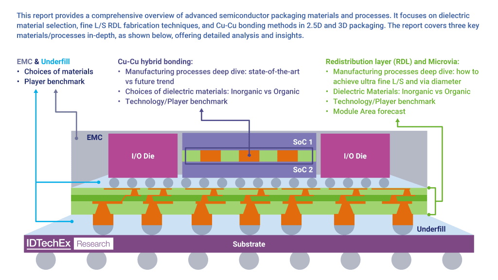
IDTechEx’s “Materials and Processing for Advanced Semiconductor Packaging 2024-2034” report is divided into four main parts, offering a structured approach to understanding advanced semiconductor packaging. The first part provides a comprehensive introduction to the technologies, development trends, key applications, and ecosystem of advanced semiconductor packaging, providing readers with a solid overview. The second part focuses on 2.5D packaging processes, delving into crucial aspects, including dielectric materials for RDL and Microvia, RDL fabrication techniques, and material selection for EMC and MUF. Each sub-section within this part presents a detailed analysis of process flows, technology benchmarks, player evaluations, and future trends, providing readers with comprehensive insights.
The report continues beyond the discussion of 2.5D packaging to the third part, which focuses on the innovative Cu-Cu hybrid bonding technology for 3D die stacking. This section provides valuable insights into the manufacturing process and offers guidance on material selection for optimal outcomes. It also showcases case studies highlighting the successful implementation of Cu-Cu hybrid bonding using both organic and inorganic dielectrics. Additionally, the report includes a 10-year market forecast for the Organic Dielectric Advanced Semiconductor Packaging Module, presented in the last chapter. This forecast encompasses unit and area metrics, providing the industry with meaningful perspectives into anticipated market growth and trends for the next decade.