On-chip interconnects have not been scaling at the same speed as transistors. When TSMC went from 20nm to 16/14nm, for example, they decided to replace the bulk MOSFET with a FinFET, but they left the interconnect stack as is. In part, interconnect scaling has been slow because companies don’t want to make too many major changes at the same time and introduce risk. Costs, of course, are also an issue. “When you’ve got ten layers of metal and let’s say six layers of those are close to minimum pitch, it gets very expensive once you start doing double patterning,” said Dr. Deepak Chandra Sekar, general co-chair of the upcoming 2014 IITC/AMC joint conference. “With the interconnect layers, people want to save litho costs. That’s one reason they are not scaling as much as they used to.”
But the major reason is that it’s difficult to make interconnects much smaller without introducing significant increases in resistivity. “If you scale down and your resistivity goes up exponentially, it can be a problem,” Sekar said. “Copper resistivity shoots up when you scale it down because of surface scattering, grain boundary scattering and interface roughness.”
The 17th annual International Interconnect Technology Conference (IITC) will be held May 21 – 23, 2014 in conjunction with the 31st Advanced Metallization Conference (AMC) at the Doubletree Hotel in San Jose, California. It will be preceded by a day-long workshop on “Manufacturing of Interconnect Technologies: Where are we now and where do we go from here?” on Tuesday, May 20.
Sekar highlighted a number of papers that will be presented this year. Many of them focus on new materials that could lead to reduced resistivity and enable further interconnect scaling. “There is a lot of excitement about carbon and carbon-copper composites eventually replacing copper,” he said. “At IITC this year, we have a couple of papers, one on graphene showing lower resistivity than copper, and then one on carbon nanotubes showing good resistivity as well. They are still a bit far out in the sense that there’s a lot more process integration work that needs to be done because these are proof of concept demos, but they show that there might be more beyond copper.”
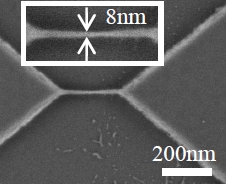
In a paper from AIST, titled “Sub 10nm wide intercalated multi-layer graphene interconnects with low resistivity,” work will be presented that demonstrates 8nm wide 6.4nm thick graphene interconnects with a resistivity of 3.2uohm-cm, which is significantly better than copper with similar dimensions. This milestone for graphene interconnect research is expected to motivate the process integration research that is required to take the technology to the next level.
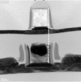
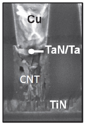
Carbon nanotubes (CNTs) have been explored as a material for vertical interconnects for many years since they can handle higher current densities than copper and offer ballistic transport. A paper from imec titled “Electron Mean Free Path for CNT in Vertical Interconnects Approaches Copper,” work will be presented that demonstrates a 5x improvement in electron mean free path for CNTs compared to previous work. The CNT mean free path of 24-74nm approaches copper. Contact resistance is improved significantly compared to previous work as well.
Another challenge to scaling of interconnects: reliability. Both time-dependent-dielectric-breakdown (TDDB) and electromigration lifetimes for interconnects drop rapidly when scaled. In work to be presented at IITC/AMC, IBM and Applied Materials will present a multi-layer SiN cap process is developed that shows higher breakdown and lower leakage compared to conventional SiCNH caps. Selective cobalt caps in combination with the multi-layer SiN cap are shown to provide a 10x improvement in electromigration lifetimes. Wrap-around cobalt liners in combination with the cap layer schemes are shown to provide a 1000x improvement in electromigration lifetimes. The paper is titled “Advanced Metal and Dielectric Barrier Cap Films for Cu Low k Interconnects.”

Of course, an alternative to making everything smaller by scaling is to go 3D. That will be addressed by a variety of papers, including one from CEA-Leti focused on 3D monolithic integration. While most of today’s through-silicon vias (TSVs) are in the 5µm range, monolithic 3D technologies offer TSVs in the 50nm range, which allows dense connectivity between different layers in a 3D-IC. In the Leti paper, such dense connectivity is shown to provide 55% area reduction and 47% energy-delay product improvement for a 14nm FPGA design. Transistor technologies that allow monolithic 3D integration are experimentally demonstrated. “When you make the TSVs smaller and smaller, you can reduce the length of on-chip wires as well by taking what’s on a single now and stacking them into two layers,” Sekar said. “That might save a lot of power and area. There’s been a lot of talk about monolithic 3D, but these are some of the first few experimental demonstrations showing that it’s possible.”