OMKARAM (Om) NALAMASU, Chief Technology Officer, Applied Materials, Inc.
As traditional Moore’s Law scaling slows down and the industry transitions to the AI era, the future of semiconductors will be driven by a new playbook for improving PPACt™ (performance, power, area-cost and time-to-market). The key elements of this new playbook are new architectures, new 3D structures, novel materials, new ways to shrink devices and new ways to connect chips together with advanced packaging (FIGURE 1).

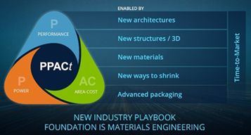
To accelerate this new PPACt playbook requires a combination of materials engineering with integrated processing, co-optimization and AI. Additionally, functional scaling will be aided by the emergence of advanced packaging solutions and More-than-Moore technologies.
Materials engineering, the ability to manipulate (analyze, create, modify and remove) materials with atomic control on an industrial scale is the foundation for semiconductor technology innovations. Beyond semiconductors, materials engineering can offer critical breakthroughs to address global inflections in fields from energy storage, engineered optics, pharmaceutical manufacturing, life science analytics and more.
This article, published in the December issue of Semiconductor Digest, details the key advances in integrated processing — along with innovations in key elements of PPACt — that are necessary to enable future device inflections to drive the semiconductor industry forward. Click here to read the full article.