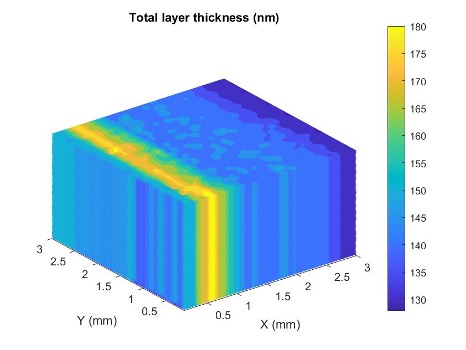
In a feature article that appeared in the March issue of Semiconductor Digest, results are presented that demonstrate the ability of new technology to evaluate both the total thickness of a multilayer structure and the thickness of each layer of samples typical of the semiconductor and of the display industry. In addition of a good repeatability which the process is guaranteed near s = 0.5%, the mapping and the massive data available with Neta technology may enhance the analyze at nanoscale for the quality of electronic components, improve yields and reduce the cost of non-quality. Nevertheless, multiple improvements are on the track, regarding both the hardware and the software with artificial intelligence implementation.
The author first describes how embedded technology in Neta’s system opens high resolution mapping or massive data acquisition. A mapping can be considered as a measurement only needs less than one second. This significantly improves the speed of acquisition and leads to much more data for control itself or potential inline inspection. After illustrating how the thickness of a layer can be evaluated, this paper focuses on another possibility offered by Neta’s system: to determine the acoustic velocity in the material. Two practical applications will then be detailed: a multilayer W-TiN-SiO2 typical from MOS devices and a multilayer SiOx-SiNx typical from display components.