YANG PAN, Corporate Vice President, Advanced Technology Development, Lam Research Corp., Fremont, CA
Every advance in technology node has required tighter control over manufacturing process variability. The most advanced processes are now creating fin widths of only 7 nm, a little more than 30 silicon atoms. Semiconductor manufacturing has crossed the threshold from nano-scale to atomic scale processing. Engineers must now be concerned with dimensional variability in the structures they create equivalent to only a few atoms. The problem is compounded by the increased number of processing steps in advanced processes like multiple patterning, which further constrains the allowable variation per step. Adding to the level of complexity and challenge are the complicated geometries in 3D NAND and finFET structures.
Controlling variability has always been a key challenge for the semiconductor industry, as it directly impacts performance, yield, and reliability, and thus, has significant economic consequences. Process-induced variability comes from multiple sources across the die, wafer, and tool. One way to gain control of variability is through the application of technologies such as atomic layer deposition (ALD) and atomic layer etching (ALE), which are inherently more precise than conventional plasma methods.
Atomic layer processing
Atomic layer processing, including both deposition and etch solutions, share some characteristics. Unlike continuous processes, they proceed in cycles, with each cycle adding or removing a finite and fixed number of molecular layers. A cycle is divided into half cycles, each of which is a distinct, self-limiting process that prepares the surface for the next half cycle. For example, in SiO2 deposition (Figure 1,2), the first half cycle involves adsorption of oxygen atoms, which is self-limited by the availability of binding sites. Excess oxygen is then purged from the chamber, and the surface is exposed to a source of silicon atoms, which react with the adsorbed oxygen to create a layer of SiO2. Again, the half cycle process is self-limited, in this case by the availability of oxygen. The self-limiting, sequential nature of ALD produces conformal films with well-controlled thickness uniformity and chemical composition, and ALD is widely used in HVM of advanced logic and memory chips.

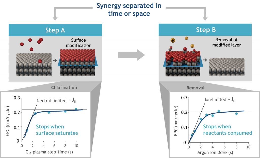

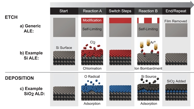
Like its deposition counterpart, ALE proceeds in half cycles that are self-limiting. In a silicon etch process, for example, the first half cycle exposes the silicon surface to chlorine, which binds to the first layer of silicon atoms and weakens their bonds to their underlying neighbors (Fig 2). The process stops when the surface is saturated, and then unused chlorine is purged. The second half cycle bombards the modified surface with argon ions, which remove the chlorine activated top silicon layer, but not the underlying silicon. When the chlorinated layer is gone, the cycle is complete and a thin layer of material has been precisely removed.
Historically, the integration of ALE into high-volume semiconductor manufacturing has been limited by its low etch rates relative to continuous etch processes. Two factors have combined to reduce the impact of lower etch rates on overall throughput. The first is the continuing decrease in feature sizes, which has reduced the amount of material to be removed and the number of ALE cycles required. The second comprises advances in ALE technology, such as rapid gas exchange techniques, which have significantly increased cycling speed. The increasing need for atomic-scale control on smaller features, has focused renewed attention on the technique. ALE also offers other important benefits, including improved directionality (anisotropy), smoother surfaces, better material selectivity, flatter etch fronts with less surface damage and mixing, elimination of pattern density-dependent loading effects and improved cross wafer uniformity.
Innovative ALE and ALD solutions
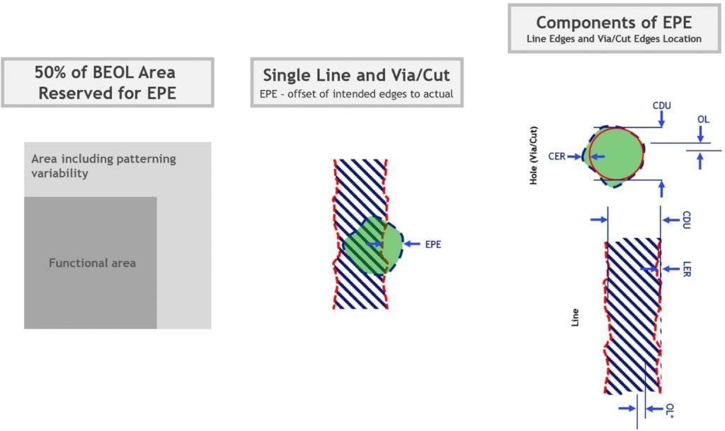
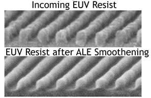
Stochastic Defects in EUV Lithography Manufacturers adopting extreme ultraviolet (EUV) lithography at the 7 and 10 nm nodes are challenged by stochastic defects. The shorter wavelength of EUV light allows it to be focused into finer patterns but also means that each photon has more energy, creates more photoacids, and exposes a larger volume of resist. EUV systems are very expensive and must deliver high throughput to compete on a cost basis with conventional (i193) lithography, so they use short exposures, low photon doses and chemically amplified resists (CAR) that can be exposed with a minimum number of photons. Random variability in the spatial and temporal distribution of photons and photoacids in the resists results in stochastic defects – essentially a statistical lumpiness that manifests in developed photoresist patterns as edge and surface roughness. Circular edge roughness (CER) and line edge roughness (LER) are components of edge placement error (EPE), which ultimately limits the extent to which feature sizes may be decreased. At advanced nodes over 50% of BEOL area is reserved for EPE; device scaling is limited by EPE scaling and requires a 30% node to node EPE reduction (Figure 3).

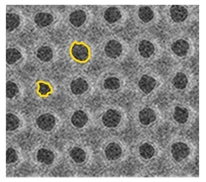
Atomic layer etch can help to mitigate the impact of these stochastic defects. Because it proceeds layer by layer in self-limiting steps, and because the steps separate the chemically active species from the energetic ions, atomic layer etch does not create the rough selvage layer found in conventional etch processes. More importantly, repeated cycles of ALE and ALD can reduce roughness caused by stochastic defects in EUV. Both bumps and divots have higher surface-to-volume ratios than a flat surface, which result in flattening of bumps during ALE and filling of divots during ALD. Stochastic defects are very small and the layers removed and deposited during this smoothing process are very thin, perhaps half a nanometer. The process has been shown to reduce CER and improve local CD uniformity in small, finely pitched holes. Likewise, it can reduce LER, improve local CDU and remove troublesome bridging defects in small, finely pitched (sub-10 nm) lines and spaces (Figure 4).
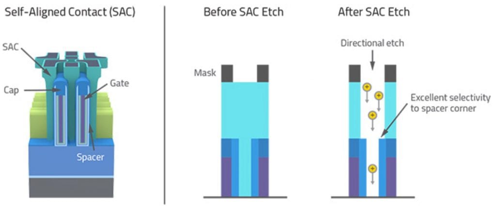
Self-aligned contact etch Self-aligned contacts (SAC) were developed to permit continued scaling by allowing the source and drain contacts to be positioned closer to the gate. In the process the gate is isolated from the source and drain contacts by lateral silicon nitride spacers and an overlying capping layer. SAC etch, which removes silicon dioxide adjacent to the spacer prior to deposition of the contact, is one of the most challenging etch processes. It must be highly selective to remove the oxide and leave the nitride spacer intact. In continuous etch processes, selectivity is created by depositing a thin fluorocarbon polymer coating. During etching the oxygen available from the oxide burns off the carbon in the polymer allowing the etch to proceed. Where the polymer overlies nitride, no oxygen is available, and etching is inhibited. The problem lies at the top corner of the nitride spacer. The sputter rate is a maximum at exposed angles of 45˚-70˚; therefore, corners etch more quickly than flat surfaces and as the corner becomes more rounded it is more difficult for the protective polymer to stick. Excessive rounding and erosion at the corner results ultimately in shorts between gate and source/drain.
ALE addresses this issue by separating the deposition of the protective layer from the etching step (Figure 5). Ions are not present during the deposition, so minimal sputtering exists during deposition and the polymer deposits uniformly over topography including corners. During the etch cycle, only ions (Ar+) are present. Oxygen in the oxide burns off the polymer and fluorine from the fluorocarbon polymer etches the oxide. When the polymer is gone, so is the fluorine, and the etching stops provided the bias power is lower than the sputter threshold for silicon nitride. On the nitride, no oxygen is present, the polymer remains mostly intact, little fluorine is available, and etching is inhibited. ALE reduces corner rounding and permits thinner polymer thickness and therefore thinner spacers. ALE’s use of self-limiting half cycles that separate the surface modification step from the active etch step offers improved control and greater flexibility than continuous etch processes. (It is interesting the note that by manipulating various process parameters it is possible to reverse the selectivity and etch nitride preferentially to oxide.)

Tungsten deposition for 3D NAND wordline 3D NAND has dramatically increased the storage density of memory devices with vertical integration. Structures that were previously confined to two dimensions, and therefore limited in density by the ability to reduce their size, are now expanding in a third dimension. These devices include unconventional geometries and very high aspect ratio features that create unique processing challenges.
Among the most challenging is filling the word-lines with conductive tungsten. 3D NAND begins with a stack of alternating oxide and nitride dielectric layers, as many as 96 layers in current generations and higher layer counts are in development (Figure 6). These are penetrated by a dense array of high aspect ratio holes and the array is separated into word-lines by high aspect ratio channels. To create the memory cells, the nitride layers must be removed and replaced by tungsten. This tungsten must be introduced through the deep (50:1 vertically) channels and then spread laterally to fill the (formerly) nitride horizontal planes (perhaps 10:1 laterally) in a super-conformal deposition with no voids. Atomic layer deposition’s ability to deposit one thin layer at a time ensures uniform filling and prevents blockages that would lead to voids.

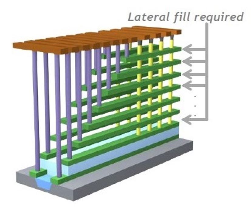
One successful approach has been to add a topographically selective inhibitor to the fill process to prevent excessive deposition in lower aspect ratio features before higher aspect ratio features have been filled. The inside out ALD process completely fills lateral (horizontal) lines without voids, while at the same time minimizing deposition in the vertical channels to enhance both electrical performance and process yield.
Conclusion
Atomic layer etching and deposition processes offer atomic scale control through the use of self-limiting reactions. Improvements in process throughput, reductions in the amount of material removed from smaller features, and increased need for atomic scale control have revived interest in ALE. The control offered by atomic layer processes assures them a growing role in current and future semiconductor manufacturing operations.