By Pete Singer, Editor-in-Chief
Onto Innovation (ONTO), created last year by a merger of Rudolph and Nanometrics, focuses primarily on optical metrology, macro defect inspection, process control software, and panel lithography. CEO Mike Plisinski believes “the company is well positioned to take advantage of the expected growth in almost every aspect of the semiconductor industry, including 5G, 3D NAND and DRAM, RF/MEMS, advanced packaging and displays.”
In presenting the company’s 2020 second quarter financial results last month, Plisinski noted, “Our product innovations are opening new opportunities of growth for the company. In the advanced nodes market, we have announced several new products that expand our leadership position in the most challenging OCD applications once thought beyond the reach of optical metrology. In the secular growth market of advanced packaging, our Dragonfly inspection system’s performance continues to be the tool of choice for the most advanced packaging technologies, targeting AI, 5G, and data center markets. Panel level packaging is increasing in importance to the industry and we were pleased to see JetStep lithography selected by new and existing customers for expansions in 2021, resulting in a record backlog for our JetStep panel lithography system.”
Acknowledging current challenges, Plisinski noted, “The Onto Innovation team continues to execute extremely well in a very dynamic environment presented by our integration, the on-going risks from COVID-19, and the US-China trade relations. Within this environment we are driving improvements in our business operations resulting in stronger financial performance and global customer support.”
In the first half of 2020, Onto Innovation introduced a suite of three new metrology products: the Atlas® 5 OCD metrology system for device metrology at the most advanced nodes; the IMPULSE® 5 integrated metrology system for CMP process control, and the Aspect® optical metrology system for very high aspect ratio features in leading edge 3D-NAND. All three systems are powered by a new software modeling engine, AI Diffract™. Also, the company’s new Element™ FTIR technology was selected by a top three memory manufacturer. And its JetStep® panel lithography system backlog grew to a record $15 million for advanced packaging of chiplets, or heterogeneous chip packages.
Optical Metrology Suite
The suite of optical metrology solutions was developed for next generation semiconductor devices to enable high-precision, high-accuracy, and high-productivity solutions for Gen6, 3D NAND, 5nm/3nm logic and advanced 1alpha DRAM devices. This new metrology suite represents the results from Onto Innovation’s newly integrated R&D team’s efforts to create a comprehensive solution set that capitalizes on its extensive experience in optical metrology and enhancements in a new machine-learning software engine for all three systems.
Kevin Heidrich, senior vice president of marketing, commented, “Our measurement data analysis from advanced logic and memory devices correlates well to our customers’ metrology lab standards, such as CD-SEM and TEM, which means they can continue to use high-speed optical metrology systems rather than switch to significantly slower, and more costly, X-ray technology.”
He continued, “For the most advanced 3D NAND devices, the challenges to measure the very high aspect ratio channel holes and word lines, with aspect ratios much greater than 80:1, are forcing customers to consider slower X-ray tools and other destructive measurement techniques. Similarly, for the most advanced DRAM and logic devices, complex transistor structures and new materials at the 5nm and 3nm nodes have customers looking at new methods of metrology for critical gate-all-around/nano-sheet processing steps. These new platforms drive optical technology to the next level, enabling its advantages of both high sensitivity and high productivity and providing customers information at the rate and quality they need for process development and high-volume manufacturing.”
3D NAND / DRAM / Logic Metrology

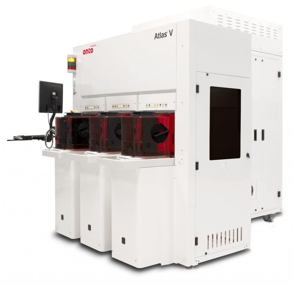
The new Atlas 5 metrology system is designed to measure several key steps that include buried features, not visible to CD-SEM and other techniques. The system delivers critical dimension measurements with the sensitivity and accuracy needed for current and next generation devices, extending the capability of optical solutions, and eliminating the need for other slower process control techniques. This includes the performance needed for advanced gate-all-around devices with measurement speeds over 100 times faster than X-ray solutions for these structures. Such speed and resolution were once thought to be beyond the limits of optical technology.

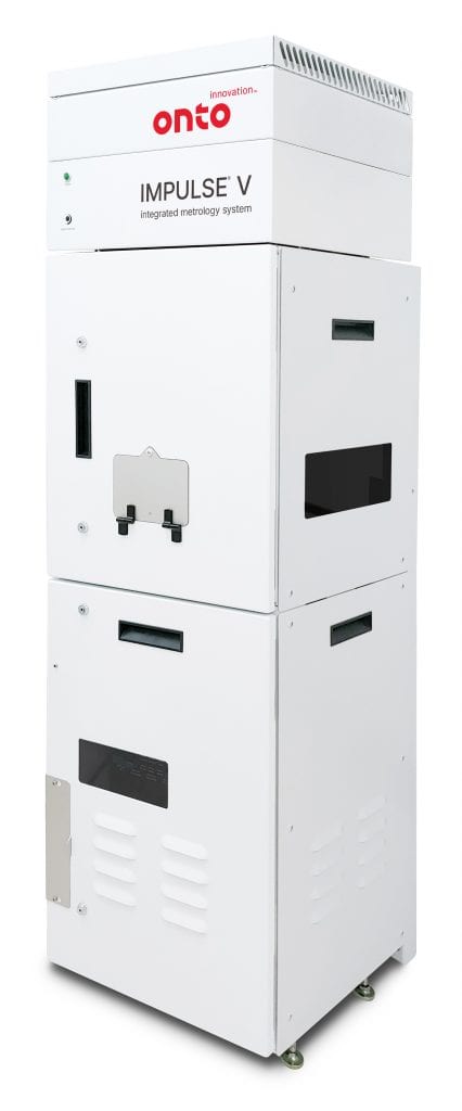
The IMPULSE 5 system enables high-productivity and high-performance integrated metrology for chemical mechanical polishing (CMP) processes, providing high-throughput, run-to-run control for critical process steps. IMPULSE 5 system recipes are inter-operable with the Atlas 5 system to facilitate production setup and optimization. The system uses the latest machine learning technology and supports on-device measurements.
3D NAND Advanced Metrology
The new Aspect metrology system is an optical platform designed to address the current and future challenges of advanced 3D NAND devices. Memory stacks already exceed 200 pairs and density increases with both layer-pair scaling and tier stacking. The Aspect system was designed with these and future architectures and scaling strategies in mind. Aspect measurements are demonstrating performance superior to X-ray systems across multiple customer devices using a novel infrared optical system that provides full profiling capability to enable critical etch and deposition control, with production-worthy speed and process coverage.
AI-Diffract Modelling Technology
AI-Diffract technology, the software analysis engine powering all three metrology systems, reduces time-to-solution by up to 90%. The new engine leverages machine learning and high-fidelity modeling to simultaneously improve metrology accuracy and speed.
Element FTIR Spectroscopy

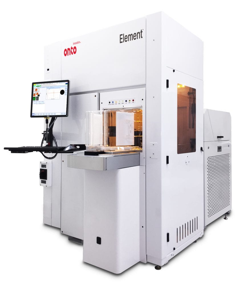
The new Element material analysis platform provides monitoring and control for dielectric thin films, measuring dopants, such as boron and phosphorous, as well as monitoring process by-products, such as hydrogen. These measurements permit correlations between material characteristics and integration variables like etch selectivity and, ultimately, parametric yield. The need for in-line monitoring of materials is expected to increase for advanced nodes as the number of dielectric and semiconductor materials used in chips increases.
JetStep Panel lithography

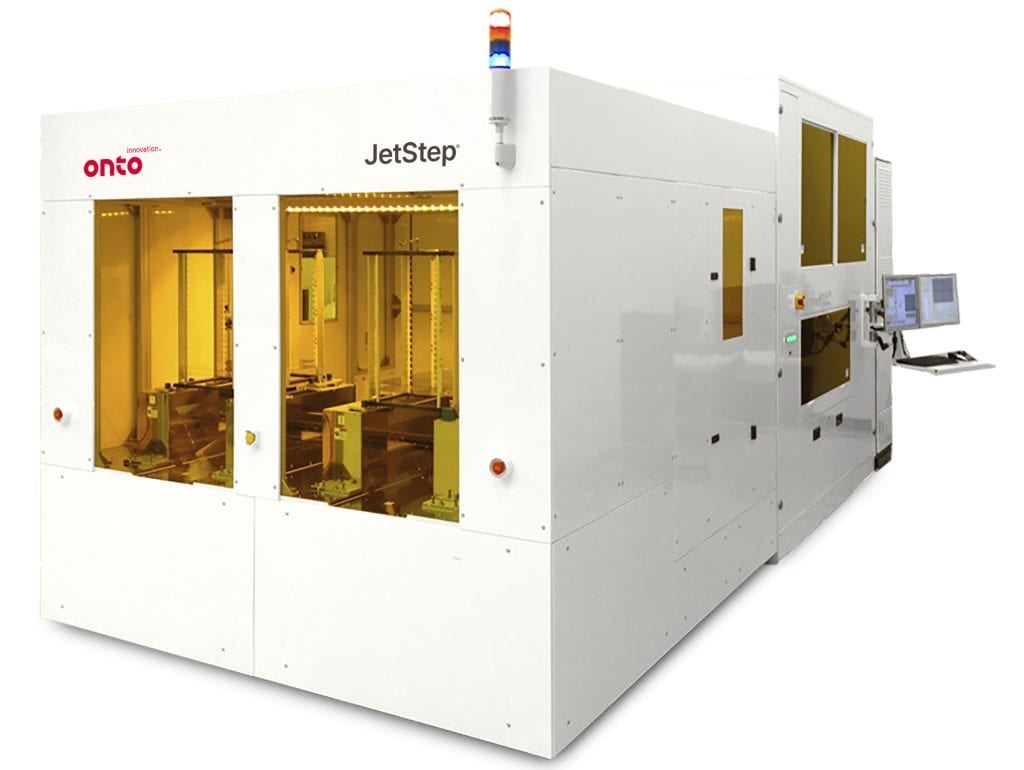
Panel lithography, which substitutes rectangular panels for the familiar round wafer form factor, offers a number of benefits, including more efficient use of corner space, better fit between die and substrate, and lower lithography cost per die on larger panels. Growth in panel lithography is being driven by the need to combine various heterogeneous chips into a single package, known in the industry as either chiplets, heterogeneous chip packaging, or system-in-package. Increasing demand for heterogeneous chip packaging is expected to come from 5G applications, data centers, AI and IoT applications. Onto Innovation announced last month that it had received multiple purchase orders for its JetStep® lithography stepper from three leading manufacturers.
“Next-generation packaging technologies require tighter overlay to accommodate a larger package size with finer pitch chip interconnects on large format flexible panels,” said Alex Chow, vice president of advanced packaging solutions at Onto Innovation. “Heterogeneous integration enables next-generation device performance gains by combining multiple silicon nodes and designs inside one package. The package size is expected to grow significantly, increasing to 75mmx75mm and 150mmx150mm, within the next few years. The JetStep lithography system offers a large exposure field that enables packages well over 250mmx50mm without the need for image stitching, while exceeding aggressive overlay and critical uniformity requirements for these packages.”
Kevin Heidrich, senior vice president of marketing commented, “Onto Innovation is delivering a complete solution to meet the challenges of panel level packaging. A combination of metrology and inspection on our Firefly® panel system, with feedforward and feedback control using our Discover® software, enables users of the JetStep lithography system to achieve higher productivity and better process control. Our combination of technology is a unique solution that can provide faster production ramps at higher yields for our customers.”