Contributed by Dick James, Fellow Emeritus, TechInsights

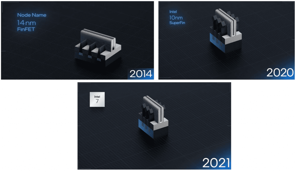
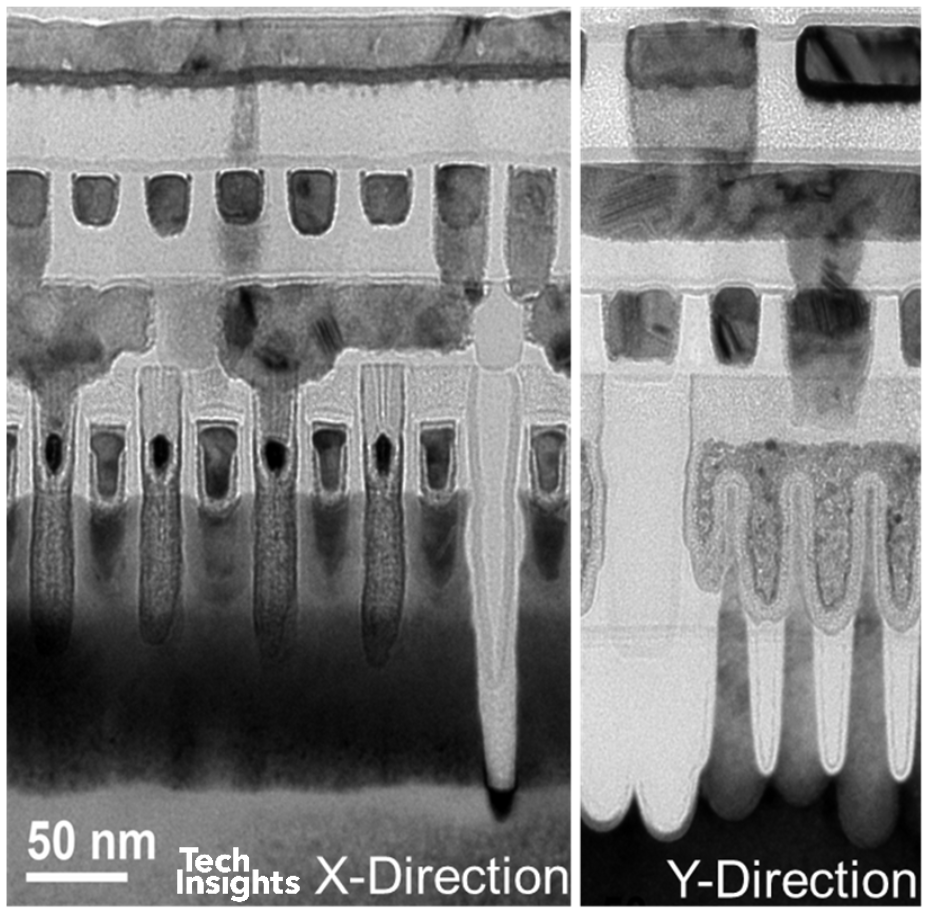
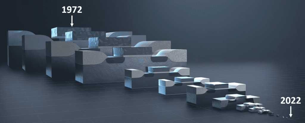
As you can see, there’s a six-year gap between the 14-nm and 10-nm nodes, and there were actually four iterations of 14-nm to get to 10-nm. In the meantime, fins became taller, more vertical, thinner, and closer together to give more drive current per unit area. We also had evolution of the gate stack to allow a greater range of threshold voltages. These are images of a 10-nm part:

Alder Lake is currently under analysis…
After running through the last 50 years of processing Pat Gelsinger looked ahead. Intel 4 and Intel 3 will continue to be finFETs. We will then see another architectural change at the 20A node (Intel’s nomenclature) to gate-all-around technology (GAA), in Intel’s parlance RibbonFETs, (nanosheets).


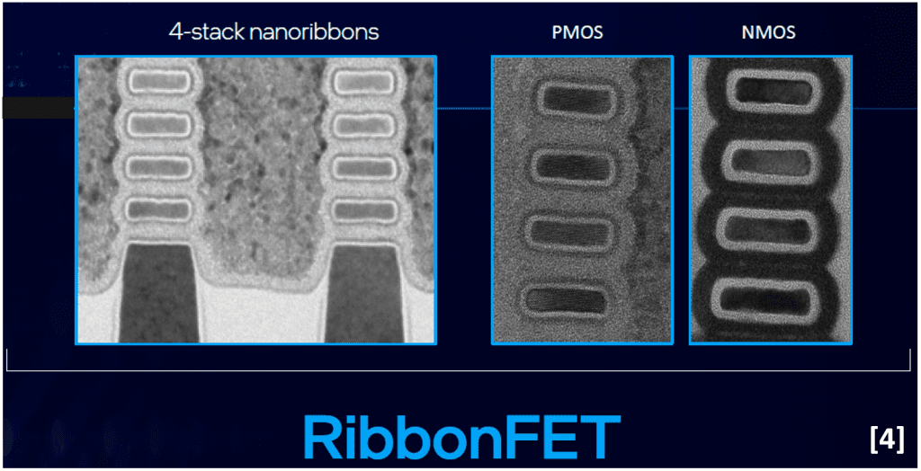
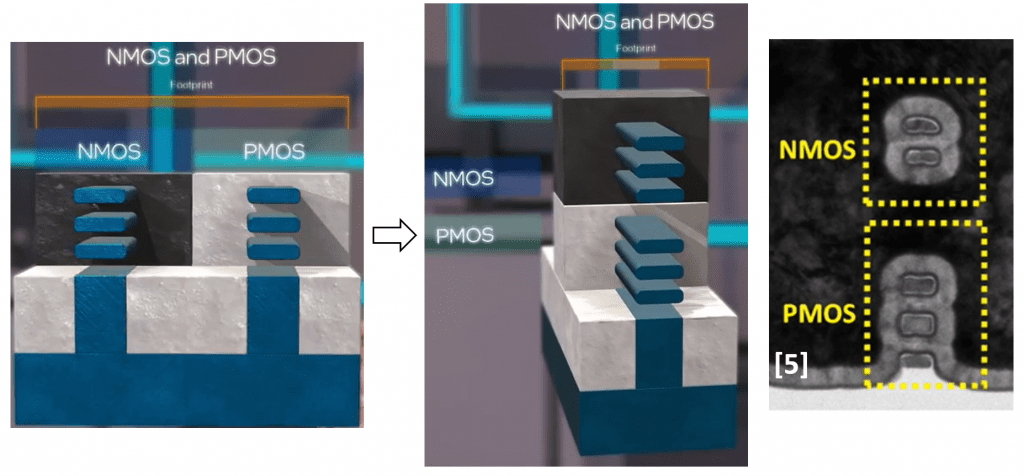
No mention was made of forksheet, imec’s introduction of a dielectric wall between NMOS and PMOS nanosheets; ultimately, to save area, we will get to stacked nanosheets, as described in Intel’s IEDM 2020 paper [5]:

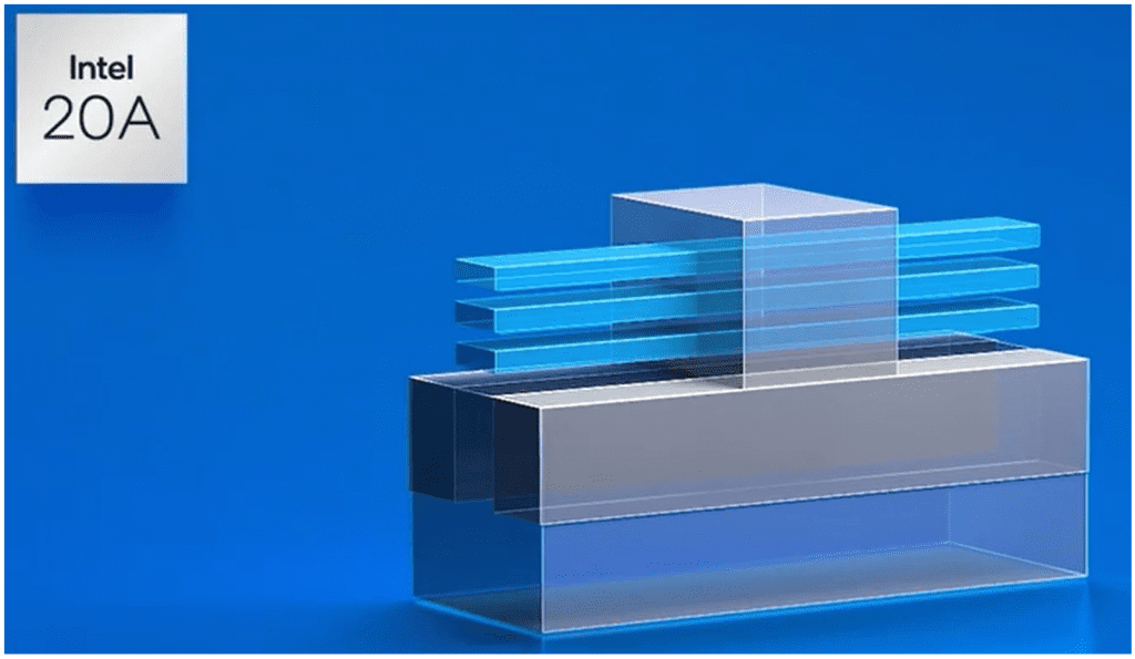
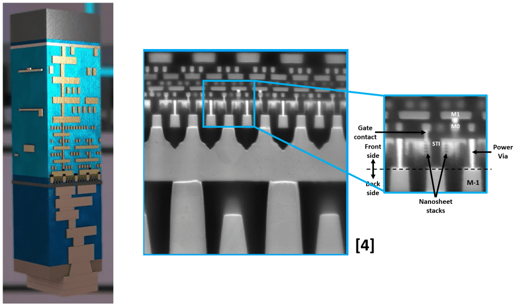
When the 20A GAA generation is launched, Intel is planning to use their PowerVia technology, putting the power delivery metallization on the backside of the die:

So in the last 50 years we have gone from the 10-micron generation to the 5-nanometer, shrinking 2000x, and to analyze them we have gone from optical microscopes to the latest aberration-corrected electron microscope.

And we still have plenty of generations to come!
References
- James, “From Strain to High-K/Metal Gate – the 65 – 45 nm Transition”, ASMC 2008
- James, “High-k/Metal Gates in Leading Edge Silicon Devices”, ASMC 2012
- Packan et al., “High Performance 32nm Logic Technology Featuring 2nd Generation High-k + Metal Gate Transistors”, IEDM 2009, pp. 659 – 662
- Intel Accelerated event 26 July 2021 https://download.intel.com/newsroom/2021/client-computing/Intel-Accelerated-2021-presentation.pdf
- C-Y Huang et al., “3-D Self-aligned Stacked NMOS-on-PMOS Nanoribbon Transistors for Continued Moore’s Law Scaling”, Proc IEDM 2020, paper 20.6, pp. 425-428