By PETER GILLESPIE, VP & GM, Semiconductor Products, Advanced Energy Industries, Inc., Milpitas, CA and DAN CARTER, Member of Technical Staff II, Advanced Energy Industries, Inc., Fort Collins, CO
In “Process Power Steps Out from the Shadows,” the first article in this three-part series, we discussed sub 14 nm technology node process challenges to highlight key drivers that are fundamentally transforming the role and importance of process power. This second article delves deeper into several critical process challenges and how process power—the radio frequency (RF) electrical energy that creates and controls plasmas—is enabling solutions in today’s IC device manufacturing.
As memory structures transitioned from planar to 3D, etch and deposition process schemes were leveraged to make ever taller stacks (up to today’s 128 and upcoming 250 or even 500+ layers), and process power became a crucial enabler. Underscoring this importance, a fab director described process power as “the new lithography” because of its increasingly essential role in patterning semiconductor device features. We will describe dynamics and process implications that are raising the importance of RF process power to the extent it is seen as fundamentally enabling in today’s semiconductor wafer device patterning.
Lithography alone no longer enough to pattern
For more than 40 years the semiconductor industry did a heroic job keeping up with Moore’s Law and doubling the number of transistors on integrated circuits (ICs) approximately every two years. This was largely accomplished using Dennard Scaling, shrinking a planar pattern to scale transistor dimensions by about 30 percent every technology generation and, thus, reducing IC area by 50 percent. However, in the past decade, Dennard Scaling alone has not been enough to keep pace, and Moore’s Law itself has been falling short.
Optical lithography has prolonged its capability to print ever-smaller features by progressing to shorter wavelength light sources. For the majority of today’s leading-edge device manufacturing, this has culminated in argon-fluoride lasers that produce 193 nm wavelength light and leverage liquid immersion to improve the optical numerical aperture (NA) and enable resolution of sub-wavelength features. The progression to shorter wavelengths slowed with the extended incubation of Extreme Ultraviolet (EUV) photolithography. Delays in the introduction of 13.5 nm EUV tools limited the widespread availability of this next progression of optical lithography in fabs until recently.
Before EUV lithography was available, novel process techniques were developed to extend 193 nm immersion lithography. Phase Shift Masks (PSM) and Optical Proximity Correction (OPC), for example, were leveraged to improve lithographic fidelity. Litho-Etch-Litho-Etch (LELE) and Self-Aligned Multiple Patterning (SAxP) were among additional innovative techniques that attempted to stretch toward Moore’s Law pace with planar shrinks while printing feature sizes significantly smaller than the lithography wavelength.
The challenge with using these techniques, and adopting EUV, is the associated near-exponential increase in cost moving from node to node. A major innovation that profoundly changed the memory technology roadmap is 3D architecture in V-NAND (and novel memory devices that could one day replace DRAM). This 3D innovation provided a wholly new dimension—vertical—to effectively multiply available memory cells per unit area (for NAND) and improve cell performance (for DRAM) while reducing the cost and complexity of lithography (FIGURE 1). While EUV lithography is now phasing into production, due to its high cost and complexity, it remains implemented only on a minority of layers targeted at the smallest features sizes, while demanding process innovations continue to be used to pattern many sub 10 nm technology node features with 193 nm immersion lithography.

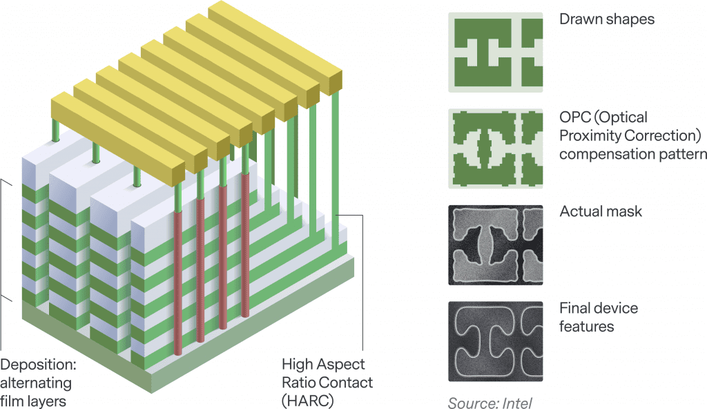
Before sub-wavelength lithography was done in practice, the photolithography mask, the photoresist pattern, and the final etched features were largely a one-for-one flow to “write” the pattern. Etch and Deposition processes for sub 10 nm technology nodes are now used to “draw-in” many of the minimum features in intermediate steps between the optical lithography exposure cycles. These intermediate processes have vastly increased the criticality of Etch and Deposition and with it transformed the role of process power.
Process challenges in a vertical world
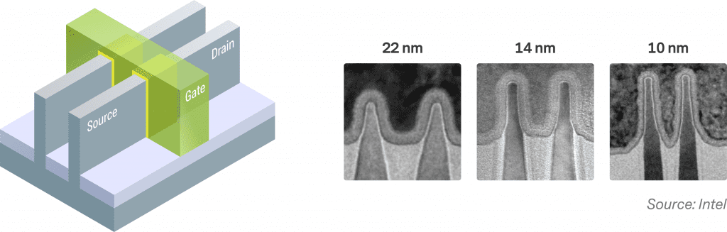
The confluence of tall vertical stacks in 3D memory devices with sub-wavelength feature lithography has brought about significant new challenges. Formation of complex transistor architectures with atomic-scale features has also raised the bar, especially in logic devices. Process power is relied upon for enabling leaps in Etch and Deposition capability to overcome these challenges and make possible continued progress in smaller, deeper HARC features and FinFET transistors.
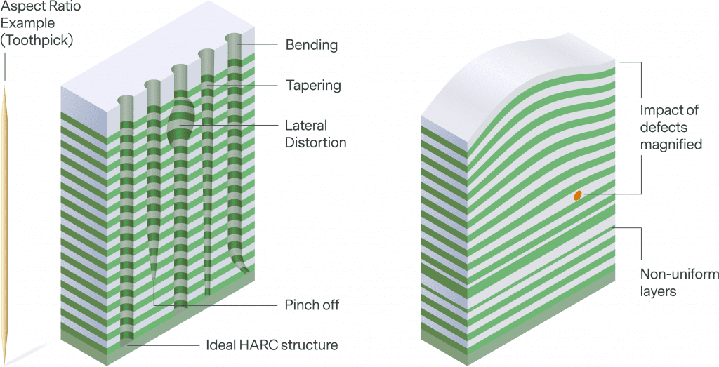
With 3D memory device architectures, the primary challenges are forming very flat layers in tall stacks (56 layers or more) and patterning small and very, very deep straight holes. To deposit layers with adequate planarity (flatness) in tall stacks, film stress optimization is required to keep the macro film surface from distorting (sometimes called “potato chipping”) as it progresses through repeated deposition cycles in the multi-film stack process. Among other process parameters, RF frequency selection and precise power control are critical to achieve the targeted thin film density and stress while ensuring rapid plasma response to the short process steps of high productivity processing. Precise power control needs to be maintained not just in terms of the power generator output but, most importantly, the actual power coupled to the plasma itself (which drives tuning network agility requirements).
For 256-layer or more NAND devices, High Aspect Ratio Contact (HARC) via (hole) or trench features can require depth-to-width aspect ratios of 50:1 or 70:1. To visualize, that’s roughly equivalent in aspect ratio to two toothpicks stacked end on end (FIGURE 2). The challenges of etching a straight hole through distinct layers—and holding it perfectly straight while ensuring it does not stop short of the bottom—are incredibly daunting. To etch these features, activated ions generated in the plasma need to get all the way to the bottom of the vias. Driving ions to the very bottom is a significant obstacle that requires specialized multi-frequency RF and synchronized RF pulsing to control ion energies and surface charging while the features are etched deeper and deeper. As in Deposition, the challenge is not only in generating the RF power, but also in matching the energy to the plasma, which requires precise power measurement and high-speed tuning of the RF power in the microsecond regime.
Power as the new lithography
As etch and deposition have been called upon to “draw” more of the device pattern, answering the following questions illuminates the profound transformation of plasma processes and precision RF power. RF power has been tapped to enable new capabilities and bring new plasma generation and control parameters to provide more “knobs” to create and control the plasma to “draw-in” patterns in these more complex 3D structures.
What’s working? RF power has come a long way since the early days of Plasma Enhanced Chemical Vapor Deposition (PECVD) and dry (plasma) Etch. The evolution of RF power delivery systems has moved in leaps from its early days of transformer and tube-based RF power supplies with fixed matching networks. The first leap was to Switch Mode Power Supplies (SMPS) and auto-tuning matching networks. SMPS enabled reliable, stable, and efficient power delivery for these plasma processes and, at the same time, the technology drastically reduced the physical size (watts/volume) for more compact configurations of process tool modules. This, in turn, meant process chamber modules could be more tightly packed on process tool platforms and resulted in higher wafer output per square meter of fab space and lower overall cost per wafer.
While there has been continued improvements in power density and price/watt, major innovations have also been keeping pace with rapidly changing plasma processing requirements. Power delivery systems further evolved in a leap to hybrid digital/analog control to deliver higher quality continuous wave (CW) RF power. More recently, power delivery systems have jumped to all-digital controls with the ability to provide frequency-tuning, complex pulsing profiles and high-speed agility to tune while pulsing (FIGURE 3). The increase in sophistication is along the lines of the progression from landline phones to analog cell phones to digital network phones to today’s smartphones. Likewise, RF power supplies have had to become “smart” to become a central enabler of the “new lithography.”

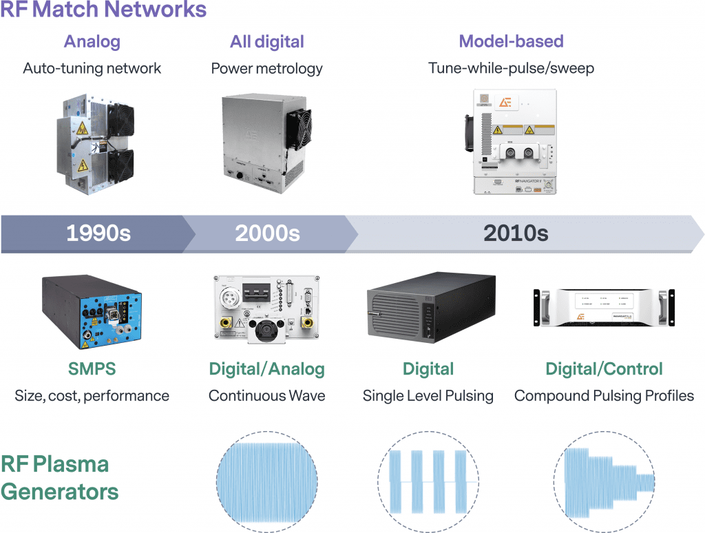
Figure 3. Evolution of RF power supplies (plasma generators) and RF matching networks. Today’s RF power delivery systems are highly sophisticated with frequency tuning, complex pulsing regimes, and agile micro-second response.
What wasn’t working? As lithography device patterning became less of a single-step process, where final device features were patterned one for one from the photoresist itself, new Etch and Deposition capabilities were required. To achieve these, the role of process power needed to be reimagined.
Despite the technical progression, for much of its use in semiconductor manufacturing, RF generators and matching networks were largely seen as “dumb black boxes.” The RF generator power level was selected and expected to simply provide constant output power at that power level. The matching network was set and expected to tune the power to the plasma continuously. However, process recipes became much more complex and increasingly included many short steps with different process conditions resulting in widely varying plasma impedances (impedance is the measure of the opposition that a circuit exerts to a current when a voltage is applied. More simply, it is the electrical “load” of the plasma). Abrupt and frequent impedance changes could not be controlled by power delivery systems that were simple dumb boxes.
A good analogy is to compare an RF generator to an automobile engine, and the matching network to a car’s transmission. When the road is largely smooth and the car speed mostly constant, the engine and transmission operate independently. In this basic case, the engine and the transmission can be unaware of each other and act as black boxes to one another. However, driving a car requires a range of speeds, road conditions, interruptions (stop-and-go traffic) and distracted drivers who want to get to their destination quickly. Car transmissions are now eight-speed, closed loop (automatic) and fully integrated to the engine, with common software continually optimizing the system for speed, changing conditions, efficiency, and acceleration.
A similar change was needed for RF power delivery systems. Etch and Deposition equipment engineers needed RF power systems, not independent “dumb” power boxes, to provide the speed of response and fully automated tuning across wildly changing process steps—with new power mode requirements added to the mix. Etch applications needed pulsing and more knobs to improve the control of the plasma environment; and matching systems needed to become more sophisticated to handle the rapidly changing plasma impedances produced by the increasingly complex process recipes and very short duration process steps.
Better separation and control of the chemical and physical properties of the plasma was required. Ion-to-neutral composition management, discrimination of chemical species energies without reducing plasma density, and improved energy distribution control were just a few of a new array of objectives emerging for RF process power. These needs drove RF power system design changes as well as new expectations for the generator and match to work together as a system (FIGURE 4).

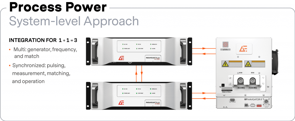
As an example, there was a need to move to new frequencies and to combine multiple frequencies (by connecting several RF generators and matching networks) on a common electrode to enable the process innovation to “draw-in” the Etch pattering steps. RF power could no longer be “one size fits all.” At the same time, while power technology and control requirements have become more numerous and more complex, it cannot be done at any cost. The sophistication needed to be implemented in way that met the all-important $/delivered-watt (power) cost targets to maintain the high productivity, high COO performance for what can be more than 150 Etch and Deposition steps for a 128-layer 3D NAND device.
Why high-speed matching? Why multi-frequency RF? Why pulsing? To form the tall memory stacks in 3D devices or the intricate 3D shapes in logic gate formation, etch and deposition processes increasingly require complex multi-step recipes. Transitions between steps in modern process recipes may involve major changes to power level, gas flows and pressure, and consequently produce sharp changes to the plasma impedance.
High-speed matching of the RF power delivery system is required to eliminate any latency that can smear the transition between steps and even “wink out” the plasma between the recipe steps due to transition discontinuity. Plasma ignition and consistency throughout the process are not only key for stability but also important to ensure predictable transitions between steps. Variations in ignition profile and delays or instability through transitions ultimately create unacceptable variation in final device features.
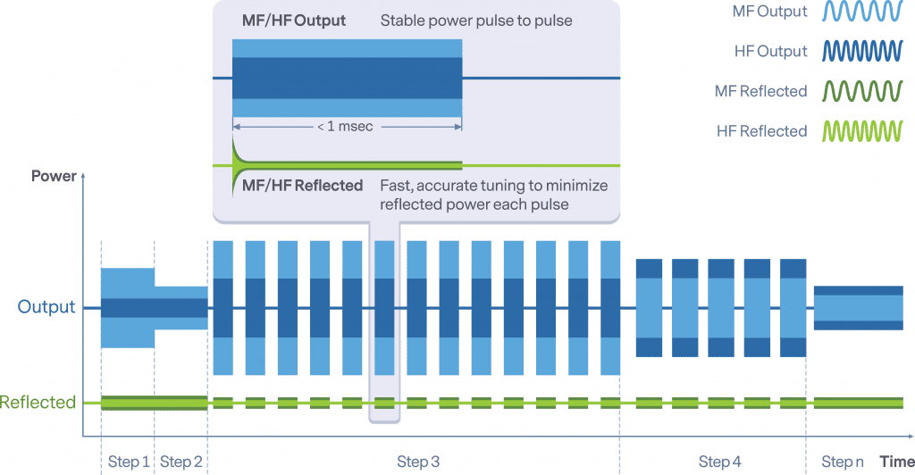
Agility and speed of frequency tuning, as well as accelerated tuning (matching) and advanced tuning algorithms, provide improved process performance, enhanced control through transitions and overall repeatability not possible in previous generations of RF power delivery systems. Collection, processing and transfer of data have increasingly become limiting factors in power system agility, driving the need for faster measurement and control systems featuring leading-edge data processing capabilities and demanding higher levels of subsystem integration (FIGURE 5).

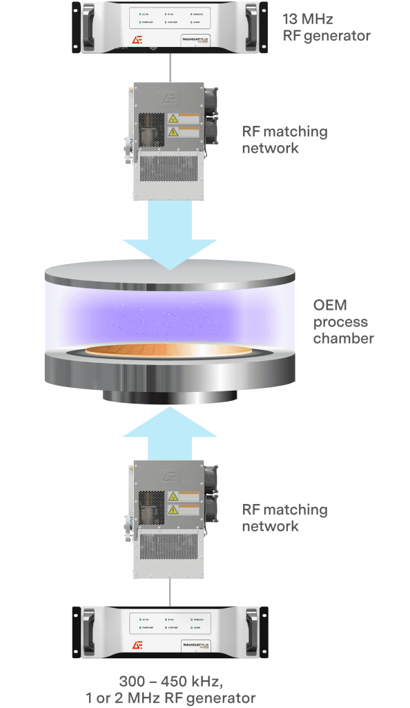

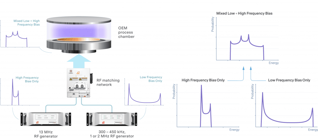
In the past, although single-frequency RF was enough for many Etch processes, the inability to adequately control the separation of plasma production from bias generation (directionality) limited single–frequency systems from etching deep holes and complex stack features. This, and other plasma power physics control parameters we will discuss later, drove the need for multi-frequency RF, usually two and sometimes three RF frequencies, to provide improved control of the substrate bias and resulting ion energy distribution reaching the wafer surface.
Medium frequency, or MF (350 – 450 kHz, 1 MHz, or 2 MHz), applied to the wafer chuck generates a broad ion acceleration bias, but is relatively inefficient for plasma generation. High frequency, or HF (13 MHz or higher), is more efficient for generating plasma density but less capable of producing high-accelerating voltages. Combining MF and HF allows efficient plasma creation with high-acceleration potentials and results in complicated but usable ion energy distribution. The multi-frequency bias approach, while higher cost and more complex than single frequency, has become necessary and is now the leading method for providing both the plasma power “horsepower” and agility to “draw” (etch) the intricate 3D device features required in today’s integrated circuits.
While combining multiple frequencies raises new challenges on its own, increasing demands for power accuracy and advanced features including pulsing and high-speed tuning, put an incredible strain on these increasingly sophisticated power delivery systems. Highly specialized expertise is required to develop and optimize measurement system speed and accuracy, leveraging algorithm and regulation accuracy, all of which require engineers to continually advance proven technologies while simultaneously driving innovation to stay ahead of the curve (FIGURE 6).

Pulsing has transitioned from “nice to have” to “vital” in leading edge device manufacturing processes and is now a mainstay in the application space. In addition to providing critical time-averaged thermal management for rising bias powers (and avoid runaway heating), pulsing has provided critical new knobs to the process engineer for controlling parameters including ion-to-neutral ratios and species discrimination (control of relative electron temperatures), surface charge accumulation, and ion energy distributions. Today, common RF pulsing ranges drop well below a millisecond at 10 percent to 70 percent duty cycles, challenging power delivery regimes which has driven RF hardware and control innovation to deliver new RF generator and matching networks.
While offering numerous advantages, pulsing also brings new challenges for the power system designer. Transitions and perturbations created by pulsing can drive major impedance excursions requiring extreme measurement speed, accuracy, and tuning agility. These transient behaviors, occurring on the nanosecond scale, challenge conventional power delivery systems and require high-speed data acquisition and state-of-the-art control systems to provide the necessary monitoring and control responsiveness.
Especially in multi-generator, multi-frequency match systems, when operating in pulse mode, all components must work in unison to be effective. A system-level approach to both design and operation has never been more essential. New features and capabilities including pulse and measurement synchronization, tune-while-pulse, high speed sub-microsecond fast tuning and model-based matching algorithms are just a few capabilities that are being integrated in the new generation of RF power delivery systems to address the new challenges.
As the semiconductor industry strives to catch back up to Moore’s Law cadence, 3D memory will continue adding layers, atomic scale FinFETS will continue to shrink, GAAFET (Gate-All-Around FET) will become a reality, and RF process power will continue to be an ever more critical enabler, “drawing-in” even more of the critical feature patterns. With continual improvements to precision and efficiency, coupled with the advent of new features including pulsing, synchronized operation, frequency tuning and model-based control, RF process power systems are leading the way in innovation and cutting-edge technology while making possible the incredible advancements seen today and developed for tomorrow’s logic and memory device processes.
A system-approach to process power delivery has become the gold standard. With the myriad features addressing an ever-expanding array of requirements, today’s power system designer, similar to the conductor of an orchestra, must ensure that each cutting-edge sub-system and feature work together in unison so the performance of the whole exceeds the sum of its parts. Bridging the understanding between power and applications will be key to the next phase in the evolution of RF process power. Accomplishing this will require out-of-the-box approaches to the design and implementation of the next generations of process power as the “new lithography.”
Powering ahead
In this article we reviewed some of the technical challenges and advances being realized in modern RF process power systems that make sub 10 nm processing possible. The transformation from “dumb” power components to fully integrated smart-power systems is being tapped to “draw” patterns in entirely new ways and earning RF power wider visibility and recognition, even to the point where some are calling it the “new lithography.” In the third and final installment, we will look at what’s next for process power and what capabilities, including beyond traditional sinusoidal RF power, are needed to ensure the industry can continue to innovate and meet the rapidly evolving challenges of a digital-first future.
General References:
Plasma Sources Sci. Technol. 8, R45–R64 (1999)
J. Appl. Phys. 97, 103304 (2005)
3D NAND/Flash processing
Microelectronic Engineering 164, 75–87 (2016)
Nanotechnology 22, 254006 (2011)
Plasma etch review
J. Vac. Sci. Technol. A 31, 050825 (2013)
Pulsed Plasma review
J. Vac. Sci. Technol. A 30, 040801 (2012)
Pulsed plasma IED and Chemistry
J. Vac. Sci. Technol. A 31, 020604 (2013)
Intel Corporation – various public presentations
Applied Materials – various public presentations and blogs
Lam Research – various public presentations and blogs