By DAVID KELF, Vice President of Marketing and Chief Marketing Officer, Breker Verification Systems, San Jose, CA
Semiconductor reliability is defined by the Oxford Dictionary of Computer Science as “The ability of a computer system to perform its required functions for a given period of time.” The more general definition is “consistently good in quality or performance; able to be trusted.” When we talk about semiconductor reliability in the modern world, particularly as it pertains to the design rather than the final physical chips, what do we really mean?
The classic reliability metric, Mean Time Between Failures (MTBF), relates to a system’s correct functional execution, and for the longest time this has been perfectly satisfactory. The more modern equivalent, the Failure-in-Time (FiT) rate is more useful for integrated circuits (ICs). However, it is becoming clear that the more general definition of reliability –– does the system maintain its quality, performance and “trustworthiness” –– is more appropriate for modern semiconductors.
A reliable semiconductor in modern systems surely must operate correctly. However, its performance and quality also need to be maintained. The system infrastructure (as opposed to function) must also continue to behave correctly. A reliable device continues to operate in adverse environmental conditions, particularly when safety is a factor, and also in adverse security conditions, where it must be impervious to malicious attack. In short, the device must have “integrity.”
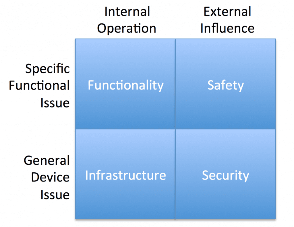
Four factors lead to device integrity: Correct functional execution, effective infrastructure operation, safe operation in adverse conditions, and secure execution in the face of malicious attack. Meeting these parameters requires additional development effort and it often falls to the verification team to ensure appropriate integrity for the given application.
From FIGURE 1, it may seem that two contributors are related to the internal operation of the chip only, whereas the other two are reactions to external influences. Additionally, two contributors relate to testing specific functional activities (i.e. positive verification), whereas the other two are related to checking specific issues will not occur (i.e. negative verification).

Functional verification is a well-understood problem, even if it continually increases in complexity. In today’s System-on-Chips (SoCs), most functional verification is performed at the block level with some functionality verified across the SoC, often as a secondary check. Driving test content that ensures effective coverage, both in terms of overall percentage and critical corner-case testing, remains a hard problem. The Universal Verification Methodology (UVM) Accellera standard and Constrained Random testing in general have improved this situation, but there is substantial opportunity for better methods.
SoC verification includes a large component of infrastructure testing. This is the task of ensuring the infrastructure of the device can keep up with the required functional operation. Infrastructure testing consists of, for example, checking that the memory configuration maintains cache coherency while handling maximum storage loads; ensuring the fabric of the device has the bandwidth to keep up with heavy on-chip communication; or that the power domains boot up quickly enough to execute an operation at short notice.
Infrastructure issues are hard to test and are an example of negative verification. The task is to make sure that, while the chip is operating, the SoC infrastructure will not fail in any way. This requires predictions of the manner in which it could fail driving stress testing where multiple activities are scheduled together. This stress testing needs to target unusual corner cases and torture the major components to maximize failure opportunity.
Safety verification requirements are epitomized by standards such as the ISO 26262 functional safety standard, which details two verification flows. Systematic verification relates to careful requirements management and proving that each requirement is fully verified. Random verification involves ensuring that the device has a low risk of failing in a harmful manner if an internal component is disrupted through an external environmental affect –– for example, a memory bit flip caused by radiation from the sun.
This second task involves the use of fault simulation, which inserts faults at key locations to ensure that they do not cause a safety hazard, or that an internal safety mechanism will stop the faults propagating. Ensuring this is performed correctly requires ultra-high coverage test content, >99% in the case of a high risk, “ASIL-D” device.
Security verification is arguably the hardest of the integrity verification components. Security verification must ensure that no vulnerabilities exist in the device that can be exploited to create an insecurity. This is dependent on the application of the device. For example, some devices might be used in safety critical applications and must be protected from hackers taking control. Other devices make use of protected keys, which should only be read through encryption mechanisms. One common security issue is the access to protected regions in the SoC, and this vulnerability affects many applications.
Security validation is another form of negative verification. Instead of checking, for example, that a protected key can be read through the crypto block, the engineer must make sure there is no other way the key can be accessed, outside of the appropriate mechanism. In addition, the engineer is testing against external effects, rather than internal operation. This combination makes verification extremely complex.
In the past, these situations would only apply to a few device applications, such as automotive. Nowadays, many devices need to worry about safety and security, and they all need to be verified against functional and infrastructure problems. The test content required for these issues appears to be different but, in fact, there is commonality across these testbenches, which may be possible to exploit.
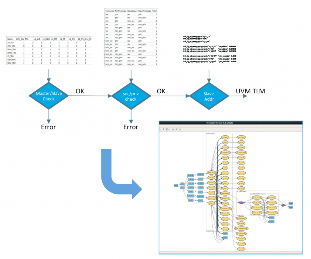
Security verification is often left to formal verification tools at the block level. The reason for this is that formal technology operates by exploding the entire state space of the design, whereupon it is easy to address queries such as “show me all the ways this key can be accessed.” At the system level, the state space is too massive to be analyzed. However, using test suite synthesis, the broad verification search space for an SoC may be constructed relatively easily, in the case of FIGURE 2, from automated table conversion. From this, test content may be generated that dives into the most complex of corner-cases. Using this method, rigorous SoC security verification may be accomplished.

In fact, all four of these verification flows can make use of this SoC specification-generated search space. The test content for these different facets of verification is converging. The intent specification may be built up using test content applied to the various blocks in the SoC, generated by apps targeting specific issues such as security, cache coherency, etc. Indeed, one end user of the technology [1] combined existing UVM functional test content with an intent scenario model for testing power domain reset with some extraordinary results in terms of coverage and schedule.
Reliability in modern semiconductors is evolving to include the four facets of design integrity. While these remain separate verification disciplines, increasingly convergence is emerging between the test methodologies. Test Suite Synthesis makes use of an intent verification search space that can be leveraged across the integrity verification problem, ultimately increasing device reliability while reducing development schedules.
Reference:
1. “Targeting Complex Power-mode Verification using Breker TrekSoC™ and Portable Stimulus at Broadcom, Inc.”, http://brekersystems.com/resources/case-studies/
About the author


Dave Kelf is vice president and chief marketing officer at Breker Verification Systems responsible for all aspects of Breker’s marketing activities, strategic programs and channel management. He most recently served as vice president of worldwide marketing solutions at formal verification provider OneSpin Solutions. Earlier, Kelf was president and CEO of Sigmatix, Inc.