SANTOSH KUMAR, Principal Analyst & Director Packaging, Assembly & Substrates, Yole Korea from Yole Développement (Yole).
The advanced semiconductor packaging industry has entered its most exciting phase. In an era of a slowing Moore’s Law, when advanced nodes no longer bring the desired cost benefit and R&D investments in new lithography solutions and devices below 7nm nodes are rising substantially, advanced packaging represents an opportunity to increase product value (higher performance at lower cost), offering advantages down both the scaling and functional roadmaps. Advanced packaging has entered its most successful era boosted by the need for better integration, the slowdown of Moore’s law and, beyond that, mega-drivers, such as big data, AI, 5G, high-performance computing (HPC), IoTs (including industrial IoT), smart automotive, industry 4.0, and data centers. The electronic hardware needed to support these mega-trends requires high computing power, high speed, more bandwidth, low latency, low power consumption, more functionality, more memory, system-level integration, a variety of sensors, and most importantly, a low cost. These new trends will create business opportunities among various packaging platforms, and advanced packaging technologies are ideal for fulfilling the various performance requirements and complex heterogeneous integration needs.
Advanced packaging has become crucial for semiconductor innovation and is essential for bridging the scaling gap between die and PCB. The semiconductor industry is developing products for scaling roadmaps and functional roadmaps, with the scaling roadmap expected to continue (7nm and below) even though only three players remain and the pace has slowed. The functional roadmap, which uses heterogenous integration and is supported by advanced packaging technology, has become more prominent. Indeed, advanced semiconductor packaging is observed to increase a semiconductor product’s value by adding functionality and maintaining/increasing performance while simultaneously lowering cost.
A variety of multi-die packaging (system-in-packages) are being developed in both the high- and low-ends for consumer, performance, and specialized applications that will address needs related to heterogeneous integration for functional performance and faster time-to-market. This places immense pressure on package suppliers, given the increasing degree of customization required for each individual customer. To fulfil next-generation hardware performance requirements, advanced packaging must press for innovations in process, materials, and equipment. Indeed, advanced packaging has accelerated the need for breakthrough technologies in substrate manufacturing, package assembly, and test engineering. Investments in next-gen manufacturing tool developments, e.g., die to die /die to wafer hybrid bonding, thermo compression bonding (TCB), LAB (laser assisted bonding), panel-level tools and substrate UV via formation, are required in order to fuel advanced packaging’s overall growth. The advanced packaging technology roadmap for I/O density vs Package size is shown in FIGURE 1.

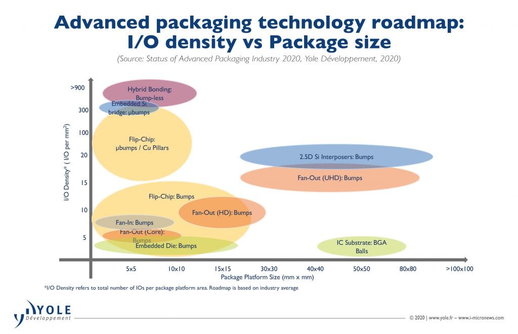
Die to die and die to wafer hybrid bonding (Cu-Cu direct bonding) is the key emerging technology for 2.5D/3D stacking and heterogeneous integration that will enable ultra-fine pitch (sub 10um) interconnect, eliminate underfill, UBM & solder plating, with significant reduction in form-factor (height). Key players have developed this technology in-house (e.g., TSMC’s SoIC) or licensed XPERI’s DBI hybrid & DBI ultra hybrid bonding technology (SK Hynix, UMC, Tower Semiconductor, etc.). As for materials, there is a desire to develop new dielectric materials, mold compounds, underfill, solder interconnects and TIMs to fulfill the stringent performance and reliability requirements demanded by next-generation hardware. Also, the need for breakthroughs in package feature-scaling requires a sense of urgency from key suppliers to the semiconductor packaging industry.
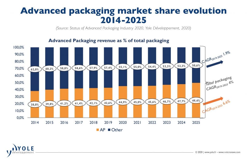
Advanced Packaging revenue will exceed traditional packaging revenue after 2025
In 2019 the total IC packaging market was worth $68B. Advanced packaging (AP) accounted for $29B and is expected to grow at a CAGR2019 – 2025 of 6.6%, reaching $42B in 2025. At the same time, the traditional packaging market will grow at a CAGR2019 – 2025 of 1.9% and the total packaging market will grow at a CAGR2019 – 2025 of 4%, reaching $43B and $85B, respectively. With a CAGR2014 – 2025 of 6.1%, the advanced packaging market is expected to more than double its revenue – from $20B in 2014 to ~$42B in 2025 (FIGURE 2). This is almost triple the expected growth for the traditional packaging market, estimated at a 2.2% CAGR2014 – 2025.
Due to the impact of Covid-19, the AP market is expected to decrease by 6.8% YoY in 2020. However, Yole expects this market to rebound in 2021, with ~14% YoY growth. The highest revenue CAGR is expected from 2.5D / 3D TSV IC, ED (in laminate substrate), and fan-out (21.3%, 18%, and 16%, respectively), as high-volume products further penetrate the market: for example, FO in mobile, networking, and automotive; 3D stacking in AI/ML, HPC, data centers, CIS, and 3D NAND; and ED in automotive, mobile, and base stations. By revenue segment, the mobile & consumer market constituted 85% of total advanced package revenue in 2019, and it will grow at a 5.5% CAGR to constitute 80% of AP revenue by 2025. Telecom & infrastructure is in revenue the fastest-growing segment (~13%) in the AP market, and will increase its market share from 10% in 2019 to 14% by 2025. Meanwhile, in terms of revenue, the automotive & transportation segment will grow at 10.6% CAGR from 2019 – 2025, reaching ~$1.9B in 2025.
Among the various AP technologies, flip-chip generated ~83% of the revenue in 2019. However, its share of the market will decrease to ~77% by 2025, whereas the share for 3D stacking and fan-out will increase from ~ 5% each in 2019 to 10% and 7% respectively by 2025. 3D stacking and fan-out will continue growing at an impressive CAGR of ~ 21% and 16% respectively, and their adoption will further increase across various applications. The 3D stacking market’s growth is led by 3D memory (HBM and 3D DDR DRAM), 2.5D interposer-based die partitioning and heterogeneous integration, 3D SoC, Foveros, 3D NAND, and stacked CIS. The fan-out packaging market is also expected to show strong growth, with players from different business models entering the market. Led mostly by mobile, fan-in WLP will grow at a 3.2% CAGR during 2019 – 2025. Embedded die, though small in market size, is expected to grow at an 18% CAGR over the next five years, with demand driven by markets like telecom & infrastructure, automotive, and mobile.
Analysis of OSATs’ financials reveal a wide gap between top 8 and rest of players
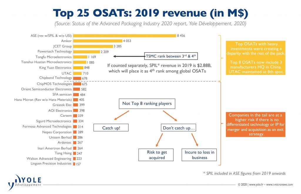
A look at the top 25 OSATs’ 2019 financials reveals growing disparity between the top 8 and the rest of the players (FIGURE 3). Top OSATs with large investments were creating a disparity with the rest of the pack. Companies in the tail are at a higher risk if there is no differentiated technology or IP for merger or acquisition as an exit strategy. In 2019, ASE became a Mega-OSAT, outranking its peers with $13.7B revenue as the SPIL acquisition was finalized and USI revenue growth in 2019 shielded it from YoY reduction compared to other OSATs such as Amkor and JCET. ASE spent ~$1.8B CapEx in 2019. This is more than 3 times the expenditure compared to next biggest OSATs: JCET ($503M) and Amkor ($472). It will not be easy to bridge the gap. TSMC remains 4th with revenue around $2.8B for 2019 as it strengthens CoWoS and InFO-x offerings for HPC and 5G deployment. Taiwanese companies continue to gain share of the OSAT market at 55% in 2019 compared to other countries as ASE rises to new heights with record revenue and capabilities. OSAT total revenue increased to $28.1B in 2019 from $27.9B in 2018, with ASE representing almost 50% of total OSAT revenue and ASE, Amkor, and JCET together representing 74% of total OSAT revenue. OSAT R&D spend in 2019 rose slightly to $1.31B from $1.29B despite sluggish demand in 1H’2019. OSAT CapEx spend in 2019 remained at 2018 levels, around $5.5B. There is a huge gap in R&D spend between top 6 players (>$50M) and other players. ASE is the only player spending in excess of $500M in R&D. 10 players have R&D spend <$10M. To maintain competitive edge requires constant innovation in technology. In the long term, players having smaller R&D investment will not be able to sustain themselves. They have limited options: either invest more in R&D or be ready for acquisitions – or to be acquired.
Players from different business models are entering advanced packaging business
There is a paradigm shift in the packaging/assembly business which was traditionally the domain of OSATs & IDMs. Players from other business models (foundries, substrate/PCB suppliers, EMS/ODMs) are entering this market and cannibalizing OSATs’ share (FIGURE 4). Advanced packaging (AP) is moving from a package substrate platform to silicon, a shift that is providing opportunities for giants like TSMC, Intel, and Samsung to flex their muscles in the AP segment, to emerge as key innovators of new AP technology. TSMC, especially, has emerged as the leader in terms of developing innovative advanced packaging platforms from fan-out (InFO) to 2.5D Si interposer (CoWoS), to 3D SoIC.
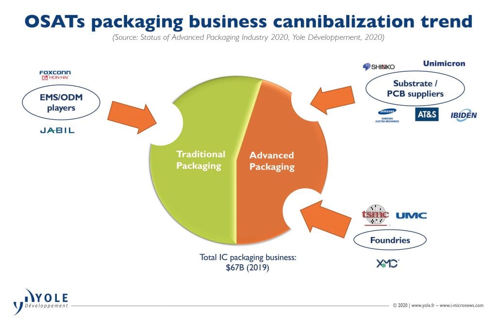
Based on current packaging revenue rankings, TSMC is #4 among OSATs. Other foundries, like UMC, SMIC, Global Foundries & XMC, are also investing in the advanced packaging technologies. Meanwhile, other top OSATs, such as ASE/SPIL, Amkor, and JCET, are investing in various advanced SiPs and fan-out technology to gauge their competition and increase their advanced packaging market share. IC substrate and PCB manufacturers, such as SEMCO, Unimicron, AT&S, Shinko, are entering the advanced packaging area with panel level fan-out packages and embedded dies (and passives) in organic substrates. Software players, like Google, Microsoft, Facebook, Alibaba, etc., are designing their own processors to gain control of the system level integration & customization and of the supply chain up to assembly and packaging level. EMS players such as Foxconn & Jabil are investing in assembly & packaging capabilities to move up the value chain to higher margin business. Top OSATs are investing in IC testing capacity to capture the test market segment. On the other hand, pure test houses, such as KYEC & Sigurd Microelectronics, are adding packaging/assembly capabilities to their service offering through M&As or by investing in R&D.
About the author


Santosh Kumar is currently working as Principal Analyst and Director Packaging, Assembly & Substrates for Yole Développement’s activities in Korea. Based in Seoul, Santosh is involved in market, technology and strategic analyses of the microelectronic assembly and packaging technologies. His main interest areas are advanced IC packaging technology, including equipment & materials. He is the author of several reports on fan-out / fan-in WLP, flip-chip, and 3D/2.5D packaging.
Santosh Kumar received a bachelor’s and a master’s in Engineering from the Indian Institute of Technology (IIT), Roorkee and University of Seoul, respectively. He has published more than 40 papers in peer reviewed journals and has obtained 2 patents. He has presented and given talks at numerous conferences and technical symposiums related to advanced microelectronics packaging.