ROBERT PAGLIARO, RP Innovative Engineering Solutions, LLC, Mesa, AZ
The advancement of silicon-based semiconductor device technology has been significantly underpinned by scientific and engineering innovations in materials, methods and machines made by the chemical vapor deposition (CVD) epitaxy experts. As ULSI and silicon based heterostructure devices shrink geometrically, transition from planar to vertical (3D), become more complex (i.e. s,trained layers) and increase in functionality, the processing requirements for the CVD of epitaxial Si, Si compounds and Ge layers have become increasingly stringent and very challenging to the established processing methods. For example, a significant reduction in the thermal budgets are required by the IEEEInternational Roadmap for Devices and Systems (IRDS) to minimize dopant redistribution and silicon migration. Exposure of the device structures to lower processing temperatures <800°C is now required. In the past, conventional ex-situ wet cleans and insitu high temperature bakes >800°C in the thermally activated processes in a CVD epi reaction chamber were used to remove adsorbed moisture and organics as well as the native oxide on the surface of the wafers. The restriction of a high temperature bake demands alternative methods to removing the surface contaminants prior to the CVD epi deposition step. Another critical requirement implemented by the IDRS for the newer device technologies is a dramatic reduction in the removal of the active area semiconductor material from the fabrication processes. All these new factors impose major challenges to the current processes of record for CVD epitaxy and wafer surface preparation.
For low temperature (LT) CVD epi processes the semiconductor wafer should ideally have a pristine hydrogen-terminated surface going into the CVD epi reaction chamber to allow the lowest possible thermal budget; therefore, anything other than hydrogen should be considered a contaminant. This pre-epi deposition surface state requires a change from using the conventional RCA wet cleaning chemistries and sequences which have been in long-standing used since the early 1970s. While the RCA wet cleans are very efficient at cleaning wafer surfaces, these peroxide-based chemistries consume silicon to create a chemical oxide passivation on the semiconductor surface. The use of alternative chemistries, methods, and/or process sequences are needed to provide a pristine hydrogen-terminated surface. In recent years the number of proposed alternatives for LT CVD epi processing has proliferated, but very few of them seem to be practical for semiconductor device manufacturing applications. The agenda for this investigation was to:
- identify a few of the practical pre-LT CVD epi deposition sequences and processes,
- identify and describe the critical steps for pre-LT CVD epi deposition, and
- identify and evaluate different pre-epi surface preparation processes/methods.
Pre- LT CVD epi surface preparation procedures, methods and processes can apply to various semiconductor compositions on a variety of semiconductor surfaces. This investigation is focused on methods for producing the pristine and stable hydrogen-terminated single crystal silicon surfaces required to achieve the specifications for LT CVD epi silicon layers. In this case, a pristine hydrogen terminated surface should be atomically flat with 100% Si-H2 (silicon dihydride) terminations. This investigation includes the challenges and the methods towards achieving and sustaining this Si surface quality up to the LT CVD Si epi deposition step.
When assessing the effectiveness of the pre-LT epi surface preparation methods and processes, the Si epi/Si substrate interface contamination level is commonly monitored to gauge the performance. The use of SIMS depth profiling on epi capped wafers has been the mainstream measurement method for this application since the late 1980s [1]. It is the measurement method used in the reference material as well as the wafers processed specifically for this investigation. There are two materials properties that are typically measured when using SIMS depth profiling to quantify the interface contamination level. They are the dose or areal density in at/cm2, and the peak concentration (Cp) in at/cm3. They are related to each other, and either or both are used at the discretion of the end user. The main chemical elements that are typically of interest to monitor for this application are oxygen (O), carbon (C), fluorine (F) and nitrogen (N). These are inherently the typical interfacial contaminants for typical pre-LT epi surface preparation sequences, and they all have higher electronegativities and surface binding energies than hydrogen [2]. The silicon surface contamination levels of these chemical elements, in any form, have a direct influence on the required thermal budget (temperature and time) of the pre-epi deposition bake to remove them. For routine monitoring (ie. SPC), it is not uncommon to only measure the oxygen and carbon since they are considered the most prevalent contaminants and good indicators if there is a problem with the pre-LT epi surface preparation sequence.
It should be noted that other inorganic contaminants are also very important to minimize for this application, but these elements and compounds were not included in this investigation because their sources and remedies are different than the intended scope.
The interface contamination elements and the defects created by them both have a negative influence on the electrical properties of the devices being fabricated. A referenced source [3] demonstrated an inverse relationship between interface oxygen dose versus the minority carrier lifetime (MCL) for a typical DHF dipped silicon wafer followed by a low temperature CVD epi SiGe deposition. For example, a wafer with an interface O dose of ~1E13 at/cm2 had a MCL of ~60 µs, while a wafer with an O dose of ~1E11 at/cm2 had a MCL of ~120 µs. This data validates that the interfacial contamination level between an epitaxial layer and the wafer surface has a deleterious effect on the electrical performance.
Practical pre-LT CVD epi surface preparation methods: integrated dry-cleaning vs. ex situ dHF last wet cleaning
Another major objective was to compare the effectiveness of an ex situ dHF wet process to the most renowned integrated pre-LT epi dry-cleaning processes being offered by the two premier single wafer CVD epitaxial system manufacturers.
In the 1990s the ITRS called for a transition from 200mm to 300mm diameter wafers. Three of the main imperatives for this transition were to:
- significantly improve the silicon wafer specifications to comply with the requirements for the newer and future device technologies,
- increase the PDPW (productive die per wafer), which reduces the manufacturing cost per die, and
- implement the FOUP (front opening unified pod) technology into the wafer handling protocol.
At the same time the requirements and specifications for the newer device technologies had also dramatically changed and became very challenging to the epi processing capabilities of the 200mm systems.
To comply, the two premier single wafer CVD epi reactor OEMs developed and commercialized 300mm single wafer CVD epitaxy systems with improved system features and capabilities that enabled the new ITRS requirements. Complementing these systems with the FOUPs with the N2 purging feature provides a very effective safeguard against the detrimental effects of exposing wafers to the cleanroom air, particularly for the queue time between an ex situ dHF last wet clean and loading the wafers onto the epi reactor. Unfortunately, for epi manufacturing facilities using smaller diameter wafers, the FOUP technology is not available. It is exclusive to the 300mm CVD epi reactors. Another major change with the transition to 300mm systems is that they were designed as cluster tools which accommodated multiple process modules to improve the wafer throughput and process flexibility. The process flexibility of the 300mm cluster tools included an option for having integrated dry-cleaning modules for LT CVD epi.
In recent years both OEMs had developed dry-cleaning process modules which became commercially available to cluster exclusively onto the premium versions of their 300mm RP CVD epi systems. Both dry-cleaning modules use remote plasma generators to create radicals from gases which are used to remove the residual surface organics and native oxide from the surface just before the wafers are loaded into the epi process chamber. The dry-cleaning process has been used “stand-alone” or in tandem with an initial typical ex situ dHF last wet clean before being loaded into the epi reactor. An ancillary benefit of the integrated dry-cleaning modules is that they do eliminate exposure of the dry-cleaned wafers to cleanroom air. For the sake of not using names the letters “P” and “S” will be assigned to the two different dry-cleaning systems for the remainder of this investigation.
It was an unsuccessful endeavor to get details for the integrated dry-cleaning process capability directly from the two OEMs for this investigation, therefore the only information that was acquired and used were from indirect sources such as published literature and private communications with people who have some level of experience with these systems/processes.
Some information for the “P” and “S” process capabilities related to this application were found in a few technical publications. While the details were not identical to this investigation, there were sections in each about the effects of different surface preparation methods on the interface contamination that were similar enough to mention.
The “P” process chamber has an integrated carbon removal and oxide cleaning process. It uses a remote plasma source (RPS) for producing fluorine radicals (F*) to remove oxide, and flowing hydrogen radicals (H*) in an inert carrier gas is used to remove carbon and carbonaceous contaminants [4].
Based on private communications, the “P” dry-cleaning process provides a minimum Si epi/Si wafer interface oxygen surface density capability of ~5E12 at/cm2, and a minimum cumulative contamination (O,C, F and N) surface density capability of ~1E13 at/cm2 for an isothermal CVD epi process at 650°C using SiH4 as the Si source gas.
The “S” process chamber also utilizes a remote plasma source to ionize NH3 and NF3 to remove oxide from the silicon surface. There was some meaningful process information related to interface contamination found in two of “S” OEM’s own technical publications.
In one publication about the “S” process, SiGe layers were deposited on single crystal silicon substrates at 700°C, 10 Torr using dichlorosilane (SiH2Cl2) as the Si precursor. In a direct comparison of the “S” process with a typical exsitu dHF dipped sample the oxygen Cp level at the interface for dHF was 2.13E19 at/cm3 while the “S” was 4.21E18 at/cm3 [5]. While this LT epi deposition process is more forgiving than the 650°C, 20 Torr silane (SiH4) process used in this investigation, it is still worthwhile to compare.
In the other publication, the “S” preclean yields a one order of magnitude higher F concentration at the interface than a typical 100:1 HF dip [6]. Since there was no F concentration or additional details about the 100:1 HF dip given in this reference, it should be noted that the F coverage on Si after using a HF dip concentration range of 0.5 to 20% is almost constant at 12% if there is no water rinse [7].
Based only the cumulative information found on the interface contamination capabilities related to using the “P” and “S” dry-cleaning surface preparation processes for LT CVD epi Si deposition, a hypothetical minimum O dose of ~5E12 at/cm2 was assigned to this method for comparison to the ex situ HF last wet cleans in this investigation.
These dry-cleaning modules are currently both single wafer CVD epi reactor OEMs’ recommended solution to meet the increasingly stringent epi/wafer pre-LT CVD epi surface preparation requirements. While they have provided a very significant improvement over just using typical ex situ wet cleans there are some notable drawbacks to this solution. They are:
- exclusive to 300mm single wafer LT CVD epi systems,
- unable to provide a pristine and stable hydrogen-terminated silicon wafer surface, because an artifact of their process chemistry is that they terminate the silicon surface with a significant density of Si-F and Si-N bonds, both of which have a significantly higher surface bonding energy than silicon-hydrides,
- add significant cost and complexity to the system,
- incur a significant reduction to the wafer throughput capacity of the system.
Ex situ-dHF last wet process and pre-LT CVD Si epi process optimization
While typical exsitu diluted Hydrofluoric Acid (dHF) last wet processes have proven to be deficient, it has already been demonstrated that an untypical ex situ dHF last wet clean system and process can provide an “as processed” pristine and stable hydrogen-terminated silicon surface [8]. Validating this was an important part of this investigation as well as the importance for optimizing all the critical pre-LT CVD epi deposition steps to constitute it as an ideal surface preparation method for this application.
Critical steps for using exsitu dHF last wet process surface prep for pre-LT CVD Si epi deposition
There are four critical pre-LT CVD Si epi deposition steps that have a significant influence on the ability to provide a pristine and stable hydrogen-terminated silicon surface using an exsitu dHF last process for the low LT CVD silicon epi deposition. It is being determined if optimizing these four critical steps, using a basic 200 or 300mm CVD single wafer epi reactor, may provide all that is required to achieve the stringent LT epi requirements. The description and recommendations for ways to optimize each of these critical steps is detailed.
(1) The exsitu dHF last wet clean process needs to be optimized to enable the removal of all surface impurities down to the bare silicon surface and terminate it with a pristine and stable H-passivation that can withstand a reasonable queue time in the cleanroom ambient without re-oxidizing. Typical ex situ dHF last wet cleans cannot provide a pristine H-terminated surface, nor is stable enough to withstand a queue time that is >20 minutes. The coverage and type of Si-Hx (mono-, di- and tri-hydrides) surface terminations on the surface strongly determine the passivation process stability. This is dictated by the dHF wet process conditions, the wafer orientation and the surface morphology (roughness).
There is a commercially available, stand alone, batch wet cleaning system which has proven to be capable to do this [8]. The key features of this unique wet process system that make it enabling are that it utilizes:
- point-of-use and integrated PPT level purification of the ultra-pure water, process chemicals and N2 for the wet cleaning, in situ-rinsing and drying of the wafers,
- an automated “dry in/dry out” technology with an integrated single vessel, cassetteless, batch wet processor with an ultra-high purity and efficient wafer drying system, and
- ultra-high purity materials, components and process conditions that minimize contamination and gaseous permeation into the process chemistry
(2) The queue time exposure of the dHF last wet processed wafer surface in the cleanroom ambient between the ex situ dHF wet clean and the loading of the wafers into the epi reactor load lock needs to be minimized. The goal of this critical step is to prevent the recontamination of the wafer surface during the queue time.
While using N2 or Ar purged micro-environments (ie. FOUP) are ideal to use during the transition from the wet process tool to the epi reactor, this investigation will focus on queue time management in a cleanroom environment.
The use of a Class 1 or 10 cleanroom environment and protocol will provide the best results.
The dilemma with cleanroom environments for this application is that they have:
- controlled relative humidity at 35-40%, which assures a significant amount of moisture in the air, and
- high organic concentrations that are generated by outgassing from the HEPA or ULPA particle filtration materials and their sealants.
So, while all the specifications of a Class 1 or 10 cleanroom environment benefit most of the semiconductor fabrication processes, at least two of the components are counter-productive for this process application.
(3) The epi reactor’s pre-LT CVD epi deposition conditions and procedures need to be optimized using the standard epi features on reduced pressure (RP) capable systems. These optimized features include utilizing:
- wafer handling carriers, transport mechanisms and process vessels/chambers made from UHP materials that do not outgas and/or contaminate the wafers in transport with foreign material
- “point of use” filters and purifiers (to < 1ppb) for the process gases, namely including the N2, H2, HCl and Si source gases
- the vacuum load lock “pump down / UHP N2 backfill” cycling feature to desorb most to all of the oxygen, moisture and organic contamination that is adsorbed onto the wafers’ surfaces during the queue time exposure in the cleanroom ambient. An extensive UHP N2 purge (at least 30 minutes) in the loadlock is considered less effective but still an acceptable alternative.
- low temperature wafer loading, sometimes referred to as “cold loading”, into the epi process chamber at <400C in H2, and then adequately purging away any residual oxygen, moisture and carbonaceous contaminants, that were introduced from the wafer handling chamber, prevents re-contaminating the wafer surface before heating up to the pre-epi bake temperature [9]. The epi process chamber pressure is also reduced while at the low loading temperature.
(4) The wafer bake, which is the last process step before the epi deposition, is the process step that is most affected by the stringent thermal budget requirements for low temperature CVD Si epitaxy. The effectiveness of the surface preparation processes and procedures up to the bake step determine the thermal workload of the wafer bake step to have a contamination free interface. Independent of the temperature and time, it is best to do the wafer bake at reduced pressure in H2 to remove any residual contaminants [9].
Study using split testing of the critical steps
As a key component to this investigation a study had been done using a juxtaposition of the critical steps prior to a typical low temperature CVD silicon epi deposition process on high quality P- (100) silicon wafers to determine if there is an ideal method to achieve a contamination free interface. Another objective of this study was to determine if a simpler and more cost-effective method could provide equivalent, or possibly better, results than the interface contamination capabilities from the “P” and “S” integrated dry-cleaning modules.
Rather than evaluating all the critical step variables for using exsitu dHF last wet process surface preparation for pre-LT CVD Si epi deposition that had already been exploited and optimized by other experts, it was determined to vary four key parameters in this study:
- a “typical ex situ HF last wet process” vs. an “optimized exsitu HF last wet process”,
- three different queue times up to 8 hours for the post-HF wet cleaned wafers to set in a cleanroom environment before placing them in the UHP N2 purged load lock of the epi reactor,
- wafer loading temperatures, and
- wafer bake temperature and time.
Other important epi processing conditions that were held constant for the testing splits were:
- all wafers were processed in basic version of an ASM E2000 RP CVD single wafer reactor,
- all wafers were purged in UHP N2 for 30 minutes in the load lock before being transferred into the epi reaction chamber,
- the wafer loading was done in H2 ambient and then pumped down to a reduced pressure,
- the wafer bake was done in H2 at reduced pressure, and
- the epi deposition was done at 650°C in H2 at reduced pressure using SiH4 as the Si source gas, which has been considered a “process standard” for characterization and troubleshooting.
A 650°C @ 20 Torr SiH4 epi deposition process recipe with a high temperature pre-epi bake (HTB) at 1100°C for 120s was used as a reactor integrity qualification. This HTB wafer bake should remove all the surface contaminants and native oxide prior to the epi deposition. Two HTB tests were done prior to running the other test splits and they did validate non-detectable (ND) oxide at the interface.
Split test information
The study identified the splits into three groups, based on the LT CVD Si epi surface cleaning process (see Table 1):
<A> “P” and “S” dry-cleaning process
<B> Typical exsitu HF last wet clean process
<C> Optimized exsitu HF last wet clean process

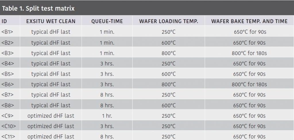
While the previously stated capabilities for method <A> are based solely on indirect sources, the data for methods <B> and <C> were empirically derived from split testing done at Lawrence Semiconductor Labs, a well established epi manufacturing and R&D facility, using conventional ASM E2000 RP CVD epi systems.
The “typical exsitu HF last wet clean” was done in a custom built manual wet bench with a recirculating and filtered etch bath, a cascading DI water rinse tank and a stand-alone spin rinser/dryer. The process sequence was a 180s etch in 100:1 (~0.5%) dHF, a 20-minute cascade rinse in DI water to 0.000% HF concentration, and a 600s heated N2 spin dry.
The “optimized ex situ HF last wet clean” was done in an APET TeraDox manually loaded, single vessel, “dry-in /dry-out” system. The process sequence was a 180s etch in premixed ~0.530% HF, a 600s in situ rinse in DI water to 0.000% HF, and a 600s heated N2 dry.
There were no other wet cleans done before either of these dHF last wet cleans. The wafers were dHF wet processed directly out of the box from the wafer supplier.
All the <B> splits used one prime grade 150 mm FZ grown high resistivity P-(100) silicon wafer per split, while the only <C> split used three prime grade 200 mm CZ grown high resistivity P-(100) silicon wafers.
The wafers were fully processed by the Lawrence Semiconductor Labs process engineering staff except for the three <C> wafers, which were dHF wet cleaned on an APET TeraDox system by an APET process engineer. Upon completion of the epi processing all the wafers were submitted to the staff scientists at EAG Analytical Lab for the SIMS depth profiling. This evaluation strategy was used to provide meaningful, expert and unbiased results.
SIMS depth profiling information and results
The SIMS depth profiling measurement results for the 11 split tests (Table 2) were intended to quantify and justify:
- the benefits of optimizing the critical pre-epi deposition steps (1) – (4) to minimize the interface contamination,
- which is the best of the pre-LT CVD silicon epi surface preparation method(s) tested to achieve the stringent LT CVD Si epitaxy processing requirements, and
- the importance and value of the an optimized ex situ dHF last wet clean.

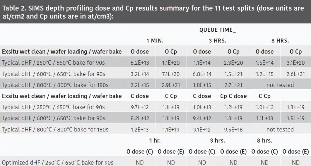
All the wafers processed for the <B> splits were measured by SIMS depth profiling for the interface O and C dose and Cp; and only in the center position of the wafer.
Split test observations and conclusions
The queue time had a largest influence on degrading the O dose and Cp at the interface for the 250°C and 600C loading temperatures, but not the 800°C. As expected, the longer the queue time the higher the oxygen doses and peak concentrations.
The wafer loading temperature had a significant impact on the O dose and Cp. The results for the 250°C wafer loading splits validated the reason for using a loading temperature <400°C. There was almost an order of magnitude difference in the O dose and Cp between each of the three different loading temperatures.
There was no noticeable affect that could be assigned to the bake time and temperature. In hindsight it may have been wise to run a split with the 250°C wafer load paired with an 800°C wafer bake.
The worst O dose and Cp results for the 250°C loading temperature (at 8 hrs. queue time) was still better than any of the O dose and Cp results for the 600°C and 800°C test splits.
Comparing the interface O dose results from the three method <C> wafers vs. all the <B> wafers, it can be concluded that <C> had the best results, primarily because of the optimized ex situ HF last wet clean.
With all three wafers from method <C> having O doses below the SIMS detection limit it is not possible to quantifiably determine how much better it is than <B>.
The carbon dose and Cp data for the split tests were all similar and lower than the lowest O dose result, which could be attributed to the other optimized conditions that were not varied.
Final comments
It is apparent that using an optimized exsitu dHF last wet process provided the closest result to a pristine and stable hydrogen-terminated silicon surface, BUT it was also essential to complement it with minimal exposure of the post-cleaned wafers to the cleanroom air, and use the “tricks” in the epi reactor to enable the most contamination free interface (by SIMS) for an isothermal bake and Si deposition process at 650°C using SiH4 as the Si source gas. The “tricks” in the epi reactor used for this study were:
1) an extended UHP N2 purge in the load lock, even though using vacuum pump down + UHP N2 backfill cycles is still preferred, and
2) low temperature (<400°C) wafer loading in H2 at a reduced pressure in the epi reaction chamber.
A typical ex situ HF last wet process is incapable of providing anything close to a pristine and stable hydrogen terminated silicon surface that would allow for an isothermal RP-CVD 650°C SiH4 epi deposition process, even with the other critical steps being optimized. It cannot compete with either of the integrated dry-cleaning modules or the optimized exsitu HF last process.
It can arguably be claimed that the interface contamination results from the optimized ex situ dHF last wet clean process sequence were equal to or better than what was documented or claimed for the interface contamination capability of both investigated integrated dry-clean process sequences. The information and data regarding the integrated dry-cleaning processes are based on indirect technical resources, the referenced processes were not under equal conditions (not “apples for apples”), and the SIMS measurements were done on different tools and by different analysts. Conversely, it is very likely that the dry-cleaning advocates made comparisons using typical ex situ dHF last wet processes, and not an optimized ex situ dHF process like what was used in this investigation. Therefore, with all these variables and many unknowns there is too much subjectivity to make any conclusions regarding which of these two methods is best.
Hypothetically, if the optimized ex situ dHF last wet clean process sequence was truely better than both of the investigated integrated dry-clean process sequences, then the requirements that come with it eliminate the need for a high end 300mm epi system, vacuum load locks, dry cleaning modules, and the FOUP technology.
Conversely, combining the optimized ex situ dHF last wet clean process/system with vacuum load locks, the enhanced cleanliness/purity features that comes with the premium versions of the single wafer 300mm RP-CVD epi systems (minus the dry-cleaning module), and the FOUP with N2 purging technology, could each contribute to further reduce the epi/substrate interface contamination capabilities.
Independent of the findings from this investigation, determining which pre-LT Si epi surface preparation solution is best for any end user is also dependent on their specific protocol, requirements and budget.
Last of all, if the ND (below the SIMS detection limit) capability becomes a process requirement, then there needs to be a different or new measurement method adopted for this application. In anticipation of this scenario, most of these wafers were initially measured {before the SIMS) by a non-contact and non-destructive measurement method called Frequency Domain-Photocarrier Radiometry (PCR). This unique all-optical method measures purely electronic carrier-wave recombination and has proven the capability to quantitatively assess the bulk and surface electrical properties of semiconductor materials, like the recombination lifetime and velocity [10,11]. While PCR has been used for semiconductors since the early 2000s this investigation provided a novel application for it. This PCR data will be correlated to the SIMS data and published in a separate technical publication.
Acknowledgements
Lawrence Semiconductor Labs (Joe Italiano, Robin Scott and their technical staff) for their overwhelming support with this investigation by providing the wafers, wafer processing, SIMS profiling measurements and technical consulting for the LT epi processes.
University of Toronto CADIPT Department (Dr. Andreas Mandelis and Dr. Alexander Melnikov) for their exceptional support by providing Frequency Domain PCR measurements on all but three of the fully processed wafers used in this investigation. This method is a very appealing alternative to SIMS and other commonly used measurement methods used for quantitatively assessing the quality of silicon epitaxy and other important front-end processes.
References
1. “Surface analysis of semiconductors with SIMS”, Trends in Analytical Chemistry, vol 3, no 5, 1984, pp 133-139, M. Grasserbauer and G. Stingeder
2. “Calculation of the surface binding energy for ion sputtered particles”, Applied Surface Science 239 (2005) 273-278, Y. Kudriavtsev et al.
3. “Oxygen in Si Epitaxial Growth: from Interface Contamination to Si/O Superlattice Engineering”, on-line PDF from SemanticScholar.org, authored by M. Caymax et al., Leuven, Belgium (IMEC)
4. “Carbon Removal and Native Oxide Cleaning on Si and SiGe Surfaces in Previum Chamber”, Solid State Phenomena, Vol. 282 (2018), pp 25-30, Fei Wang et al (ASM)
5. “Effects of Growth and Surface Cleaning Conditions on Strain Relaxation on SiGe Films beyond a Critical Thickness on Si (001) Substrate”, ECS Transactions, 33 (6) 523-528 (2010), Jeongwon Park et al. (AMAT)
6. “Advantage of Siconi Preclean over Wet Clean for Pre Salicide Applications Beyond 65nm Node”, 2006 IEEE International Symposium on Semiconductor Manufacturing, pp 393-396, Jianxin Lei, et al. (AMAT)
7. “Native oxide Growth and Hydrogen Bonding Features on Chemically Cleaned Silicon”, The Physics and Chemistry of SiO2 and the Si-SiO2 Interface 2″, (1993) pp 177-186, Masataka Hirose et al. (Hiroshima University)
8. “Surface preparation technology provides pristine and stable hydrogen passivated semiconductor surfaces”, Solid State Technology, Nov/Dec 2017 issue, pp 27-30, R. Pagliaro Jr.
9. “Low Temperature Pre-Epi Treatment: Critical Parameters to Control Interface Contamination”, Solid State Phenomena, Vols. 145-146 (2009) pp 177-180, Roger Loo et al. (IMEC)
10. “Infrared photocarrier radiometry of semiconductors: Physical principles, quantitative depth profilometry, and scanning imaging of deep subsurface electronic defects”, Physical Review B 67, 205208 (2003) pp 1-18, Andreas Mandelis et al.
11. “Method of Photocarrier Radiometry of Semiconductors”, US Patent 7,045,786 B, issued May 16, 2006, Andreas Mandelis et al.