By Chris Jones, Edwards Vacuum
In the last post to this blog, we introduced the theme of sustainable manufacturing, which will be our ongoing focus. We described the evolving framework for limiting carbon emissions and reviewed the vocabulary we will use going forward. This post will briefly overview the materials released off-site during semiconductor manufacturing – what they are, where they come from, and where they go.
In most places around the world where semiconductors are manufactured, emissions and waste management are highly regulated to ensure the community’s safety and minimize negative environmental impacts. In the United States, the Clean Air Act (CAA) defines criteria pollutants, sets national emission standards for hazardous air pollutants, and limits greenhouse gas emissions into the air. The Clean Water Act (CWA) defines limits for priority pollutants released into the water. The Resource Conservation and Recovery Act (RCRA) and Toxic Substance Control Act (TSCA) govern solid wastes. Similar regulations exist in other countries. The regulators also define a detailed classification schema to facilitate reporting and ensure appropriate handling and treatment for different hazardous materials.
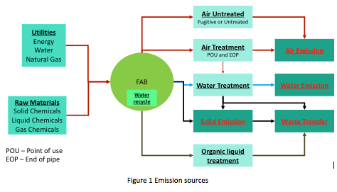
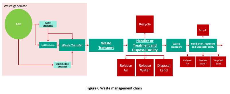
Inputs to the semiconductor manufacturing process include utilities (electrical power, water, and natural gas) and materials (solid, liquid, and gaseous chemicals). All major manufacturing facilities recycle/reuse water but ultimately release treated wastewater, organic liquids, gaseous emissions, and solid waste. Air emissions include treated air (treated at point-of-use or end-of-pipe) and untreated air (clean enough to release without treatment or fugitive air that has unintentionally escaped treatment). Water emissions consist of treated water, from which hazardous pollutants have been removed to maintain compliance with the CWA. All other solid and organic liquid waste is transported off-site (Fig 1).

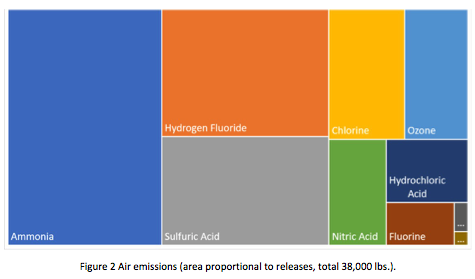
The Toxics Release Inventory (TRI) is a publicly available database (https://www.epa.gov/toxics-release-inventory-tri-program) containing information on toxic chemical releases and other waste management activities in the United States. For example, TRI data for one specific fab in 2020 indicated that all manufacturing waste was either released to the atmosphere (25%) or transported off-site (75%). Permit-compliant treated wastewater was discharged to publicly owned treatment works (POTW). The same fab released 38,000 pounds of compounds to the air, of which the primary components were ammonia, sulfuric acid, hydrogen fluoride, hydrogen chloride, chlorine, nitric acid, and ozone (Fig 2).

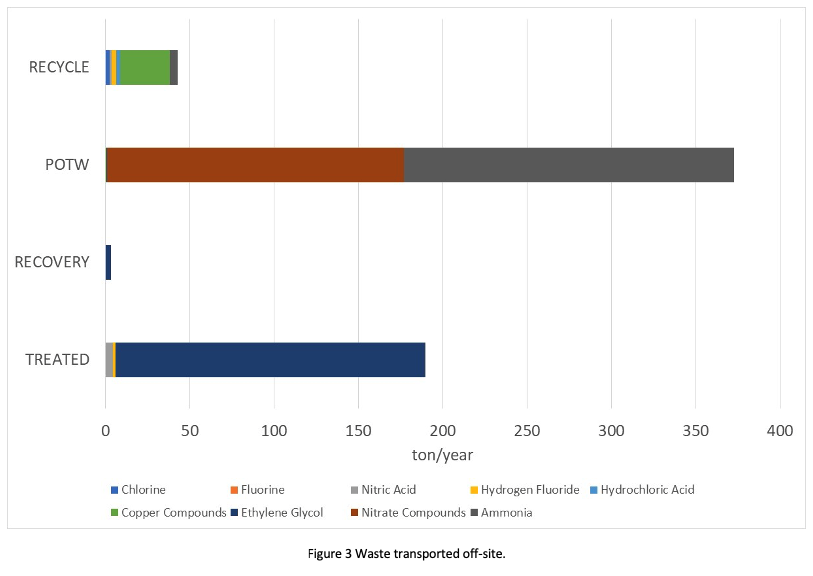
More than 630 tons of waste was transported off-site annually (Fig 3). Ammonia and nitrate compounds were mainly discharged to the POTW, along with some copper and copper compounds. Waste management companies treated ethylene glycol and recycled copper compounds.

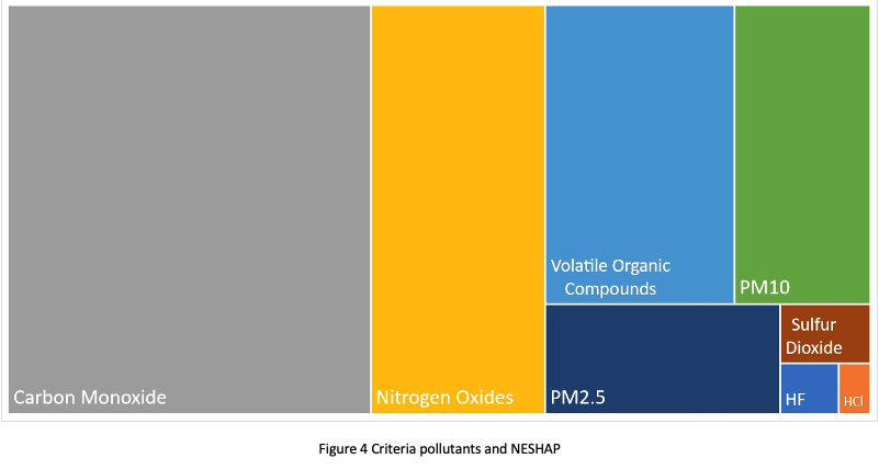
The Environmental Protection Agency has established national ambient air quality standards (NAAQS) for the six most common air pollutants. These are carbon monoxide, lead, ground-level ozone, particulate matter, nitrogen dioxide, and sulfur dioxide, known collectively as “criteria” air pollutants. In addition, national emission standards for hazardous air pollutants (NESHAPs) have also been established for other hazardous pollutants. In 2019, a semiconductor fab released 285 tons of criteria air pollutants and HAPS in one year (Fig 4). The EPA classifies any source with actual or potential emissions of more than 100 tons per year of a criteria pollutant as a major source. Lower thresholds may apply in non-attainment areas where air quality is worse than the NAAQS. Major source thresholds for “hazardous air pollutants” (HAP) are 10 tons/year for a single HAP or 25 tons/year for any combination of HAPs.

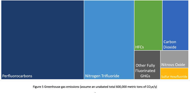
There is an obligation to report all greenhouse gas (GHG) releases above the US’s threshold limit of 25,000 metric tons carbon dioxide equivalent (CO2e). Any residual emissions from the abatement equipment are included in the site releases. The regulations demand that the fab operator report unabated emissions (0% DRE) if the fab fails to test the DRE performance of abatement or fails to maintain the equipment as per the manufacturer’s guidelines. By way of example, , a semiconductor manufacturer reported about 600,000 metric tons of emissions per year of GHG (Fig 5). PFCs dominated the reported releases, along with carbon dioxide sources from generators, POU abatement fuel burners, and boilers.


The take-away
Although semiconductor manufacturing generates significant air emissions and liquid and solid waste, the industry has historically been conscientious in its efforts to treat or dispose of its waste safely. It has also given priority to reducing emissions and other environmental impacts. As awareness of human effects on the environment has grown in recent years, manufacturers and their stakeholders have prioritized sustainability. This post has reviewed emission sources and sketched out the waste management process. By way of illustration, we have offered several examples of waste output from semiconductor manufacturing. Subsequent posts will explore the development of more sustainable strategies and business models.