Timon Evenblij, imec, Leuven, Belgium
Memory is an important topic in the design of computer systems. At imec, we develop multiple emerging memory technologies, for standalone as well as for embedded applications. Options range from MRAM technologies for cache level applications, new ways for improving DRAM devices, emerging storage class memories to fill the gap between DRAM and NAND technologies, solutions for improving 3D-NAND storage devices, and a revolutionary solution for archival type of applications – in order to meet the memory requirements of the future zettabyte era.
In this article, I will limit myself to memories based on Dynamic Random-Access Memory (DRAM), which are typically used as the main memory in a computer system. For this type of memory, I want to paint a bigger picture, from an architectural point of view. After giving some background information, I will take a look at different memory standards and their generations, to identify some common trends and bottlenecks.
Before diving into different DRAM flavors, let’s start with the basics, based on a lecture from prof. O. Mutlu [1].
Background

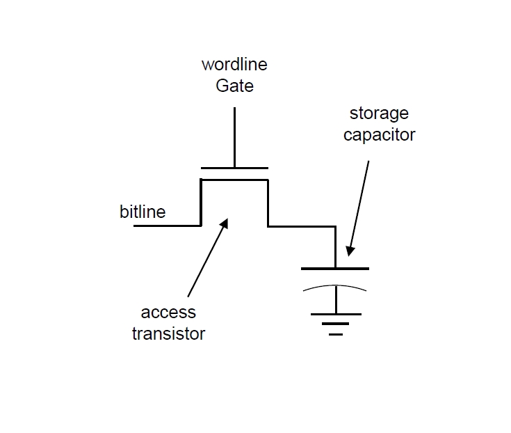
Bit cell Any memory is built up using bit cells, which is the semiconductor structure that stores exactly 1 bit, hence its name. For DRAM memories, the bit cell consists of a capacitor and a transistor (Figure 1). The capacitor is used to store a charge, and the transistor is used to access the capacitor, either to read how much charge is stored or to store a new charge. The wordline is always connected to the transistor gate, controlling the access to the capacitor. The bitline is connected to the source of the transistor, reading the charge stored in the cell or providing the voltage when writing a new value to the cell. This basic structure is very simple and small, so manufacturers can process a very large amount of them on a die. One disadvantage is that the single transistor is not very good at keeping the charge in the small capacitor. It will leak current from or to the capacitor, making it lose its well-defined charge state over time. This problem is circumvented by periodically refreshing DRAM memories, which means reading the content of the memory and writing it back. Attentive readers might have noticed as well that when a charge is read from the capacitor, it is gone. After reading a value from a DRAM cell, the value should be written again. This is what gives the name ‘Dynamic’ to DRAM.
Accessing arrays of bit cells Many cells can be combined into large matrix-like structures. Long wordlines and bitlines cross each other and a bit cell is processed at each intersection. Putting a voltage on a wordline selects all corresponding cells, which will put their charge on their respective bitlines. This charge will change the voltage of each bitline very slightly. This slight change is detected using sense amplifiers, structures who will amplify a small positive change in the voltage to a high voltage (representing a logical 1), and a small negative change in the voltage to zero voltage (representing a logical 0). The sense amplifiers store the logical values into a structure of latches, called the row buffer. The row buffer acts like a cache holding the values just read from a single word line worth of bit cells, since the values are lost in the cells when they are read. The process of sensing is an inherently slow process, and the smaller the capacitors and the longer the bitlines, the longer this process takes. This sensing time is what dominates DRAM access times, and it has remained about the same value in the last decades. The ever-increasing available bandwidth for each DRAM generations is enabled by exploiting more parallelism in DRAM chips, rather than decreasing the cell access time. But before going deeper into this issue, let’s take a look at how a memory system is build using a lot of these bit cells. The architecture I describe here is for typical desktop systems using memory modules. For other DRAM flavors, the concept of a module is not used, but most of the architecture can be described with the same terminology.
DRAM architecture On the processor, there is some part of the logic dedicated for a memory controller. This logic handles all accesses from the CPU to the main memory. Processors can have multiple memory controllers. Memory controllers have 1 or more memory channels. Each memory channel consists of a command/address bus and a data bus (which is 64 bits wide in the default case). To this channel, we can connect 1 or more memory modules. Each memory module consists of 1 or 2 ranks. A rank contains a number of DRAM chips that combined provide enough bits each cycle to fill the data bus. In the regular case where the data bus is 64 bits wide, and each chip provides 8 bits (so-called x8 chips), a rank would contain 8 chips. If there is more than 1 rank, the ranks are multiplexed on the same bus, so they cannot put data on the bus at the same time. The chips per rank operate in lockstep, which means they always execute the exact same commands and cannot be addressed separately. This is important for the following: Each chip consists of several memory banks, which are the large matrices of bit cells with word lines, bit lines, a sense amplifier and row buffer, as I introduced earlier. Since chips in a rank operate in lockstep, the term memory bank can also refer to the 8 banks across the 8 chips of the same rank. In the first case we might use the term physical bank, while in the latter case the term logical bank is preferred, but this terminology is not always clearly defined in literature.
While smaller structures exist in memory banks, I won’t talk about them in this article. With all the previous terminology, we are now able to talk about different DRAM flavors and generations, and how they improve upon each other. Again, let’s start first with regular DRAM modules for PC’s.
DRAM standards
Regular DDR DRAM memories have existed for a very long time, but I won’t give you a complete history lesson. I will go shortly go back to single data rate (SDR) memories, before jumping into double data rate (DDR) generations. What we need to know about SDR, is that the interface and data bus was clocked (IO clock) at the same frequency as the internal memory (internal clock). This kind of memories are limited by how fast the internal memory can be accessed.
The first DDR generation aimed at transferring two data words per every IO clock cycle, the first word on the rising edge of the clock and the other on the falling edge of the clock. The designers did this by introducing the concept of prefetching. A so-called prefetch buffer was inserted between the DRAM banks and the output circuitry. It is a small buffer that can store 2 times the number of bits that would be put on the bus each cycle in the original SDR design. In case of an x8 chip, the prefetch buffer would be 16 bits in size. We call this a 2n prefetch buffer. With a single internal read cycle of a complete DRAM row of e.g. 2k columns, there is more than enough data to fill this prefetch buffer. In this prefetch buffer, there is enough data to fill the bus with a word on both the edges of the clock.
The same prefetching idea was applied with DDR2, now with a prefetch buffer of 4n. This allows the designers to double the IO clock compared to the internal clock, and still fill the data bus every cycle with data. DDR3 takes the same idea further, again doubling the prefetch (8n), and the IO clock, now 4 times the internal memory clock.

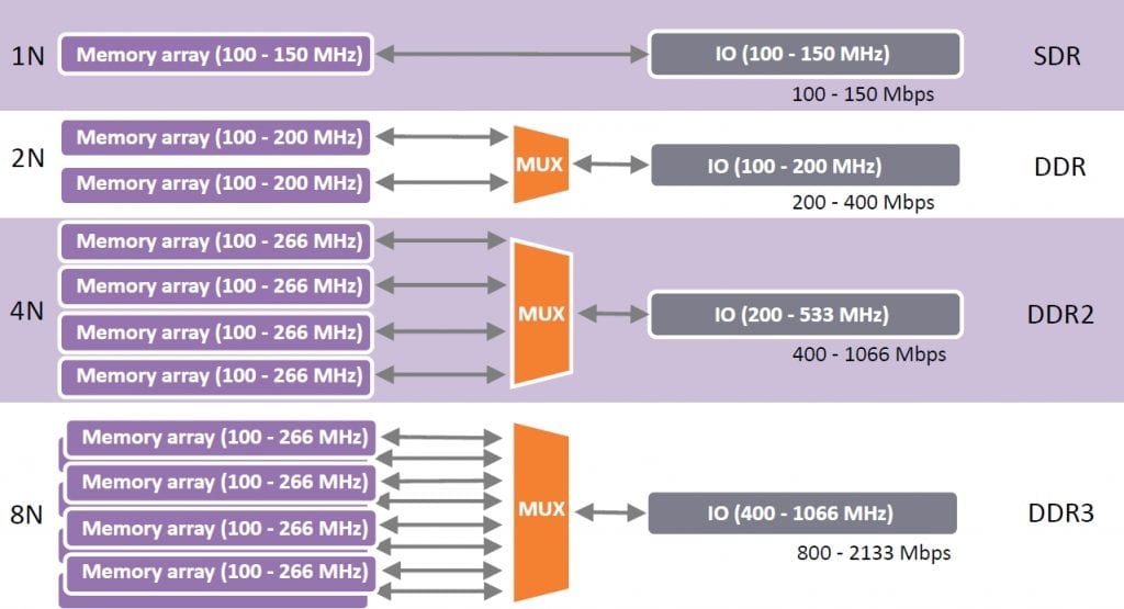
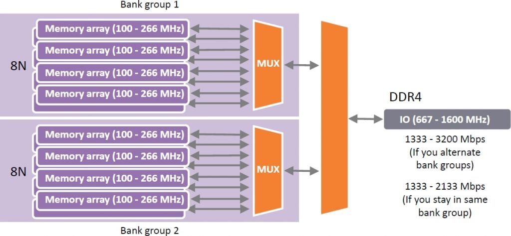
However, there are limits to how far we can keep pushing the same idea. Doubling the prefetch buffer another time to 16n would mean that for each read command, 16 times 64 bits would be transferred towards the processor. This is twice the typical size of a cache line, the basic unit of data used in processor caches. If only 1 cache line would contain useful data, we would waste a lot of time and energy by transferring the second cache line. Thus, DDR4 did not double the prefetch, but applied another technique: bank grouping. This technique introduces multiple groups of banks, with each group having its own 8n prefetch buffer, with a multiplexer to select the output from the right group. If the memory requests from the controller are interleaved, so that they access different groups on successive requests, the IO speed can again be doubled, now 8 times the internal clock speed.

So, what is next for DDR5, which also aims to double the IO speed? Well, DDR5 aims to borrow a technique already implemented in LPDDR4, which we call channel splitting. The 64bit bus is divided into 2 independent 32bit channels. Since each channel now only provides 32 bits, we can increase the prefetching to 16n, which will result in an access granularity of 64 bytes, which is exactly equal to the cache line size. The increase in prefetching allows again for a higher IO clock speed.
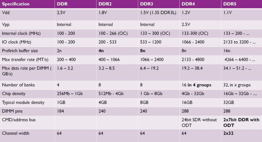
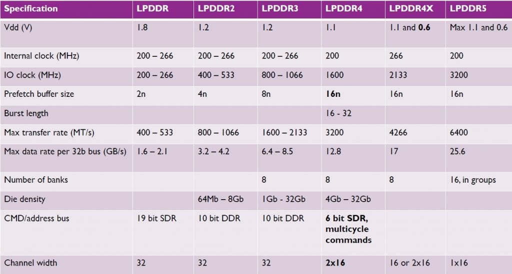
Of course, increasing the IO clock speed is not as easy as just having enough data available to fully use the bus in each cycle. Multiple challenges related to high frequency signals have presented themselves such as signal integrity, noise, and power use. These are solved by several techniques, such as on-die termination, differential clocking and general closer integration of memories with the processor (Table 1). These techniques originate mostly from other DRAM flavors, namely LPDDR and GDDR, but I will focus more closely on integration.

LPDDR LPDDR stands for low power double data rate. The main idea behind this standard is to lower the power usage of the memory, as the names implies. This is done in multiple ways.
The first distinction with regular memories is how the memory in connected with the processor. LPDDR memories are closely integrated with the processor, either soldered on the motherboard, close to the CPU, or increasingly common, provided as package-on-package directly on top of the processor (mostly an SoC in this case). Tighter integration allows for less resistance in long wires connecting the memory to the processor, resulting in lower power.

The second distinction is the channel width. LPDDR memories don’t have a fixed bus width, although 32-bit busses are most common. This is a smaller bus compared to regular memories, saving power. Also, a lower voltage is used in the memories, which also has a big impact on the power use. Finally, the standby power of memories is greatly reduced in LPDDR memories, by optimizing the refresh operation with various ideas, such as temperate adjusted refresh, partial array self-refresh, deep power-down states and more. I won’t dive deeper into these techniques right now, but generally they trade off some response time with a lower standby power usage, as the memory needs time to ‘wake up’ from a power saving more before being able to respond to the request.
Table 2 shows the generational changes in LPDDR memories, implementing the same techniques to improve performance, as discussed in the previous section. However, LPDDR4 was the first standard to introduce 16n prefetch and channel splitting, while LPDDR5 is expected to be the first LPDDR standard to introduce bank grouping.

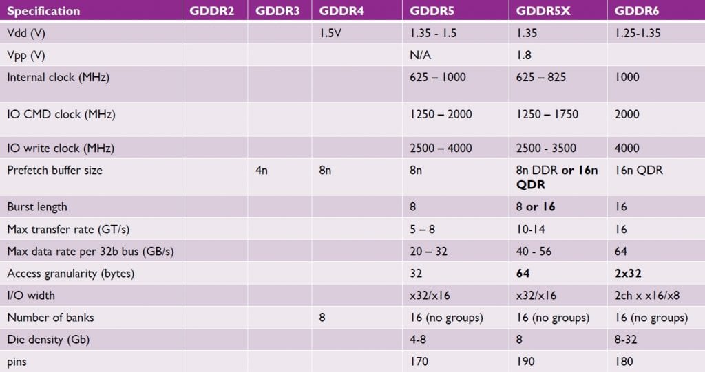
GDDR GDDR stands for graphics double data rate, implying the standard is for memories intended to be used in graphics cards. Nowadays, they are interesting for any application with a high bandwidth demand, as this is what they are focused on. GDDR memories are also pretty closely integrated with the processor, in this case the graphics processor, by being soldered on the PCB. These are not implemented on top of the GPU, as it would be hard to reach the desired capacity in this case, and because the generated heat would be hard to cool in this scenario. Each GDDR chip has a larger width compared to the typical DDR chip (e.g. 32 bit), and each chip is connected to the GPU directly, without being multiplexed on a fixed 64bit sized bus. This means having more GDDR chips on a graphics card means having a larger bus. Eliminating the multiplexing of connections also allows for higher frequencies on these connections, enabling an even higher IO clock frequency in GDDR memories. The higher IO clock speeds are enabled by higher internal read speeds, by using smaller memory arrays and bigger periphery, reducing the memory density of GDDR chips. The tight integration means the final capacity of a graphics card is even more limited, since only 12 GDDR chips can fit closely around a large GPU.
Throughout the GDDR generations (Table 3), the same techniques as in DDR are used to improve the memory bandwidth. The first GDDR standard was GDDR2, which was based on DDR. GDDR3 was based on DDR2. GDDR4 barely existed and can be skipped here. GDDR5 is based on DDR3, and was and still is very popular. It implements differential clocking and can keep two memory pages open at once. GDDR5X is a mid-generation performance enhancement for GDDR5, introducing a quad data rate (QDR) mode with 16n prefetching, at the cost of a larger access granularity, which is less of a problem for GPUs. GDDR6 then splits the channel, like LPDDR4. This provides two independent smaller channels on the same bus, enabling a smaller access granularity, making the 16n prefetch QDR mode standard. Yes, this means GDDR6 could probably be more aptly named GQDR6.

The 3D revolution
All things previously discussed all happened without any of the 3D revolution currently happening. 3D can mean a lot of things in semiconductor terminology, but for now it mostly refers to the use of trough-silicon-vias (TSVs), which are vertical interconnects in the dies, that can be connected using microbumps between the dies. Two dies put on top of each other can now potentially communicate with a lot of very small vertical interconnects. This enables completely new designs and architectures. Let’s look at the counterparts to the DRAM flavors discussed before. The most famous one is High Bandwidth Memory (HBM), which is the 3D counterpart to GDDR. Hybrid memory cube (HMC) was a proposed 3D counterpart intended for similar applications as general DDR, developed by Micron, but was cancelled in 2018. Wide I/O is a JEDEC standard pushed by Samsung for the 3D counterpart to LPDDR memories in SoCs, but I have not heard about real implementations yet.
HBM
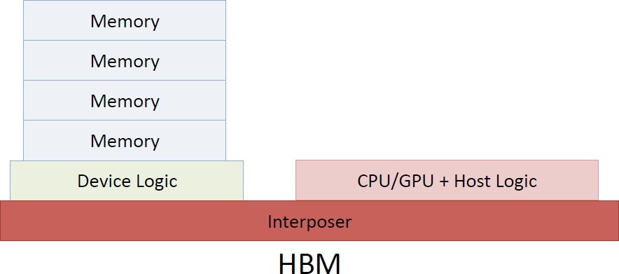
HBM has a lot in common with GDDR. The memory chips are also integrated closely with the GPU. They are also not put on top of the GPU, since we still need a lot of capacity and we need to cool the chips.
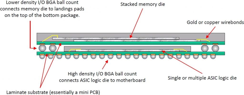
What is different then? First, instead of putting the memory chips on the PCB close to the GPU, they are put on an interposer connecting the chips with the GPU (Figure 5). Today, typically a passive silicon interposer is used, which is a large silicon chip, but without any active components: it only has interconnects on it. The advantage of this interposer is that we can route a lot more parallel interconnects on it that don’t consume a ton of power. Hence, a very wide bus can be created, which was impossible on a PCB. This interposer, while fairly simple to create, still is a large piece of silicon, so it introduces a higher cost.

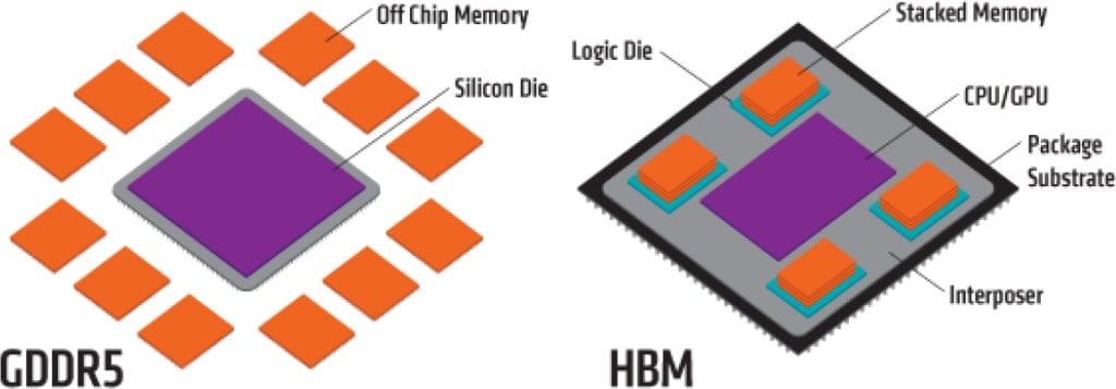
Secondly, memory chips can be stacked, enabling high capacities on a small area in the horizontal plane (Figure 6). These chips have a large amount of TSVs, connecting the chips in the stack with each other and the logic die at the bottom. This logic die is then again connected with the wide bus on the interposer, enabling the high bandwidth between memory chips and GPU. In fact, the bus is wide enough, that the IO clock of the memory chips can be relaxed to lower frequencies. This, together with the very short interconnects to the GPU, enables a much lower energy per bit (around 3x) when using HBM.

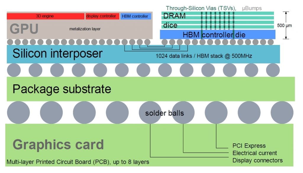
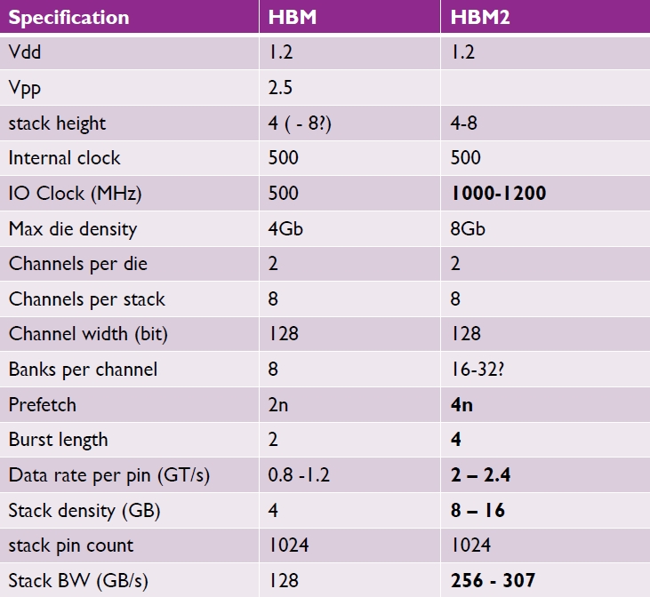
Table 4 shows some of the key specs of the HBM generations. Currently, HBM2 memories are available. Interestingly, Samsung recently announced HBM2e memory, where their chips go out of standard specification by having a larger capacity per die (16Gb) and increasing the data rate even more (410 GB/s per stack). See the article in Reference [2].

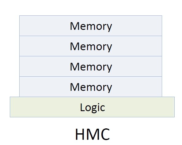
HMC
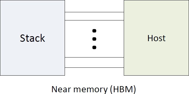
Although Micron cancelled their efforts on the standard of HMC, I still want to give it at least a few words. HMC was the 3D counterpart to regular DDR memories, especially in future servers. This perception was not always clear in the industry. HBM really focuses on bandwidth, it needs to be closely integrated, trading off capacity and expandability. This is called a near memory. HMC focused on capacity and easily plugging in more memory stacks into a server, the same way more DDR memories can easily be plugged into a motherboard with free slots. It provided the loose integration required for high total system memory capacity. This is sometimes called far memory (Figure 7).


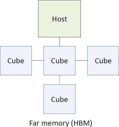
Next to this similarity, HMC is the standard that differs the most from DDR, more than any other standard mentioned in this article. Instead of using the DDR signaling across a bus, it uses memory packets, sent on high speed SerDes links between the processor and the memory cubes. This way, daisy chaining cubes is possible, enabling even higher capacities with limited interconnects. Also, a memory controller was completely integrated in the base die of each cube, instead of being on the CPU die as in DDR, or being spread over both the GPU and the memory stack, as in HBM (Figure 8).


Wide I/O
Wide I/O is the 3D counterpart to LPDDR memories, opting for extreme integration to reach the lowest power possible. The memories are expected to be integrated directly on top of SoCs, using TSVs to connect directly to the CPU die. This will enable extremely short interconnects, requiring the least power of any standard. Also, depending on the density and size of the TSV technology, very wide busses are also possible. However, this extreme integration will also require TSVs in the SoC, which consumes a lot of precious logic area, and thus is very costly. This is probably a big reason why I haven’t seen any commercial products yet with this technology. Perhaps interesting is that the first Wide I/O standard implemented an SDR interface, but the second-generation standard shifted to a DDR interface.
Conclusion
Hopefully you have understood more of the intrinsic design trade-offs different DRAM flavors have made and will make in the future. In the end, each standard implemented the same ideas to improve the bandwidth each generation, including techniques such as larger prefetch buffers, bank grouping, channel splitting, differential clocking, command bus optimizations and refresh optimizations. Each standard just has its own focus, whether it is a) capacity and flexible integration (DDR and HMC), b) the lowest power (LPDDR and Wide I/O), or c) the highest bandwidth (GDDR and HBM).
It is interesting to see what 3D technology brings to this table, for each target market. 3D integration allows for wide busses and low-resistance, low-noise interconnects. While the technology and benefits are quite revolutionary, the architectural principles and trade-offs are in most cases actually not that different.
References
2. <https://www.anandtech.com/show/14110/samsung-introduces-hbm2e-flashbolt-memory-16-gb-32-gbps>.