By DICK JAMES and JEONGDONG CHOE, TechInsights, Ottawa, Canada
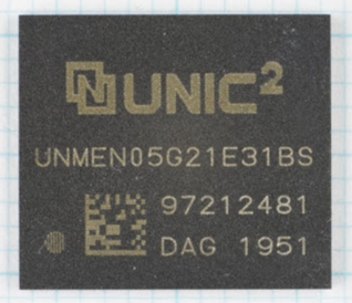
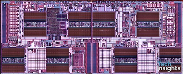
Recently TechInsights acquired a UNIC2 UNMEN05G21E31BS 32 GB eMMC part, containing a 256-Gb TLC 3D NAND flash die fabricated by YMTC in Wuhan, China (FIGURE 1).

There are two major reasons that this part is of particular interest to the industry, one commercial, the other technical – it is the first 3D-NAND device to come out of a Chinese-owned company; and it uses wafer bonding to stack the peripheral circuitry with the memory array, so the bit density is not reduced by adding die area adjacent to the memory.
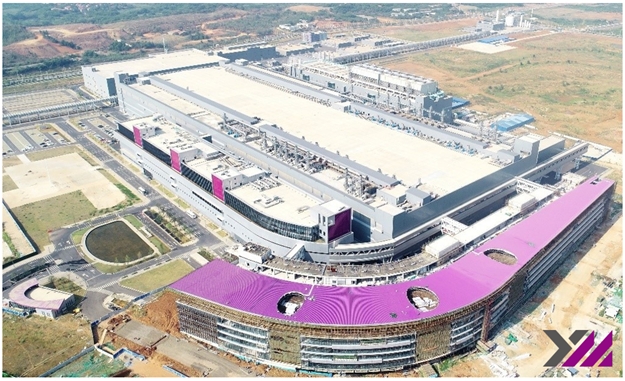
YMTC (Yangtze Memory Technologies Co.) was founded in 2016 by China’s state-owned Tsinghua Unigroup, which owns 51% of the company. Other shareholders include China’s National Semiconductor Industry Investment Fund (known as the Big Fund). YMTC uses the 300-mm fab built by its wholly owned subsidiary XMC in Wuhan (FIGURE 2). XMC historically worked closely with Spansion (now Cypress) manufacturing their NOR flash, using charge-trap storage. YMTC successfully designed and manufactured its first 32-layer 3D NAND flash chip in 2017, which is available only for a few USB customers in China.

This part is their second-generation 3D-NAND technology, using “Xtacking” to bond the peripheral circuitry face-to-face with the memory array instead of alongside it.
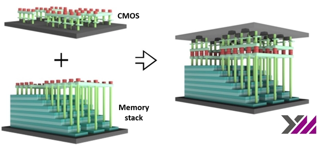
The peripheral circuitry for memory cell operation and I/O is formed on a separate wafer using a CMOS logic technology node suitable for the desired I/O speed and functions. The finished memory array wafer is then connected to the periphery wafer by billions of metal VIAs (Vertical Interconnect Accesses), shown in FIGURE 3.

The part was discussed at the Flash Memory Summit in 2018 (FMS2018), and won the “Best of Show” award (We would have included a link to the paper, but it was not included in the proceedings.)
In addition to minimizing die area, the technology was claimed to improve latency; “At present, the world’s highest 3D NAND I/O speed is targeting 1.4Gbps while the majority of the industry is offering NAND I/O at 1.0 Gbps or below. With our Xtacking® technology, it is possible for NAND I/O speed to reach up to 3.0 Gbps, similar to I/O speed of DRAM DDR4. This is going to be a game changer in the NAND industry,” said Simon Yang, CEO at YMTC.
The die image in FIGURE 4 is taken from a product brief which can be obtained through the TechInsights blog posted on March 12 [1].

Die size is not quoted, but bit density is given as 4.41 Gb/mm2, which for a 256 Gb die gives us ~58 mm2, and from that we can get dimensions of ~12.0 x 4.8 mm.
The bit density compares well with the Micron/Intel 64L CuA (CMOS under array) 256 Gb TLC at 4.40 Gb/mm2, and is noticeably denser than the Samsung 64L 256 Gb part (3.42 Gb/mm2). That’s almost a 30% bit density improvement over the conventional Samsung layout with the peripheral circuitry next to the array.
FIGURE 5 shows the memory die imaged from the back side. We can see that there are eight 32-Gb blocks, and if we use our estimated die length of 12 mm as calibration, each block comes out at ~1.5 x 1.7 mm (2.55 mm2), or 12.55 Gb/ mm2 for an array block, and the 16-Gb sub-blocks are ~0.95 mm2. Memory array efficiency is >90%.

In the 3D stack we see 73 gate layers (wordlines) in the vertical NAND string, likely 64 functional gates, plus five dummy gates and four select gates (1 Source SG and 3 Drain SGs). The SEM cross-sectional image in FIGURE 6 is also from the product brief, with some added annotations:

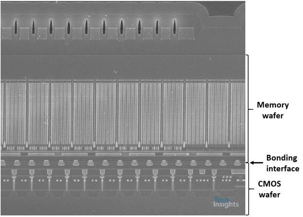
This image is inverted compared to the schematic above, with the CMOS structure below the memory stack. The CMOS wafer uses four metal layers, and the array wafer has three, but there is also a post-wafer-bonding aluminum metal layer, with passivation layers above, at the top of the image.
That looks like a conventional bond pad or RDL layer, which raises the question of how it connects to the peripheral circuitry at the base of the stack – TSVs? We can see from the die photo that all the 60 bond pads are on the top edge of the die, so if those have TSVs under them, not too dense, certainly nowhere near those used in image sensor chips.
Consequently, the top-die image above is purely the aluminum pattern on the back of the memory wafer, and not the pattern of the memory array below. It looks like two large blocks, but as we’ve seen that’s not the case.
After preliminary analysis of the process flow and interconnection, we found the TSVs (or TSC, Through Silicon Contact) in each array and block edge area, which is quite a unique process design. To do this, the NAND array die (substrate) is the die that has been thinned down for the TSV (or TSC) process.
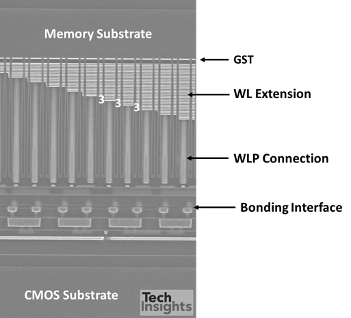
FIGURE 7 is an enlarged segment of the cross-section in Fig. 6 with our annotations.

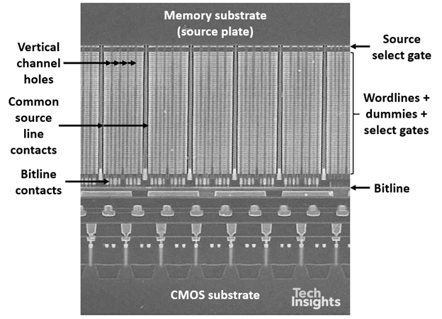
The wordlines, select gates, and bitline contacts are tungsten, and the common source line (CSL) contacts are polysilicon/TiN with tungsten caps. Between the CSL slits we can see there are nine vertical channel (VC) holes, including one dummy hole in the center. Bit-line pitch is 40 nm, so self-aligned double patterning (SADP) is likely used.
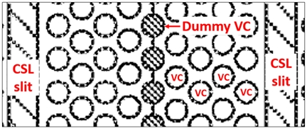
In this cross-section the VCs are not perfectly in the polishing plane of the sample, so we see the tops and bottoms of the VCs alternating. The layout of the VCs actually makes it impossible to get them all in one plane, since they are offset from each other, as shown in FIGURE 8 from a YMTC patent:

It was thought that the wafer bonding used the DBI® (Direct Bond Interconnect) technology from Xperi, but XMC (now part of YMTC) claims that they independently developed their own method for stacking wafers.
At FMS2018 a couple of pictures were shown which give us more views of the structure; FIGURE 9 is of the staircase at the edge of the memory array. It is inverted with respect to the SEM images above, and they have helpfully added the number of wordlines per step, showing us that there is one dummy wordline at the top, and what looks like three individually-masked select gates. It is worth noting that there is over a year between the FMS2018 talk and the production part being analysed, so it is possible the structures are not exactly the same.

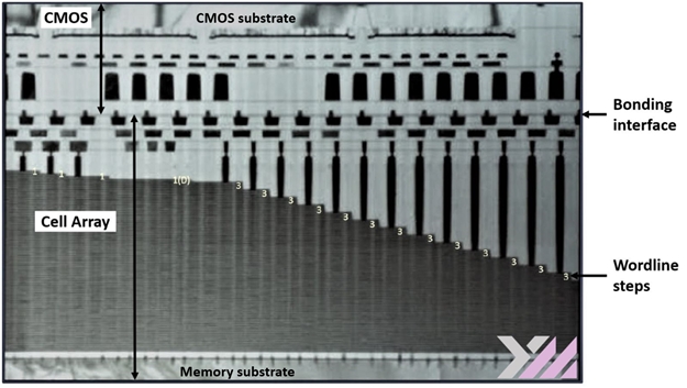
However, as we can see in the SEM image in FIGURE 10, they have almost the same process and design in the WLP connection (staircase) area in the production sample.

It’s not specifically mentioned in any of YMTC’s pronouncements, but the XMC link to Cypress charge-trap storage in NOR flash makes it seem likely that their 3D-NAND is also charge-trap based, along with most of the other manufacturers.
Another image, FIGURE 11 illustrates the TSVs, although they are calling them through-array contacts (TACs) in all the array areas and through-Si contacts (TSC) in most of the array/block edge areas.

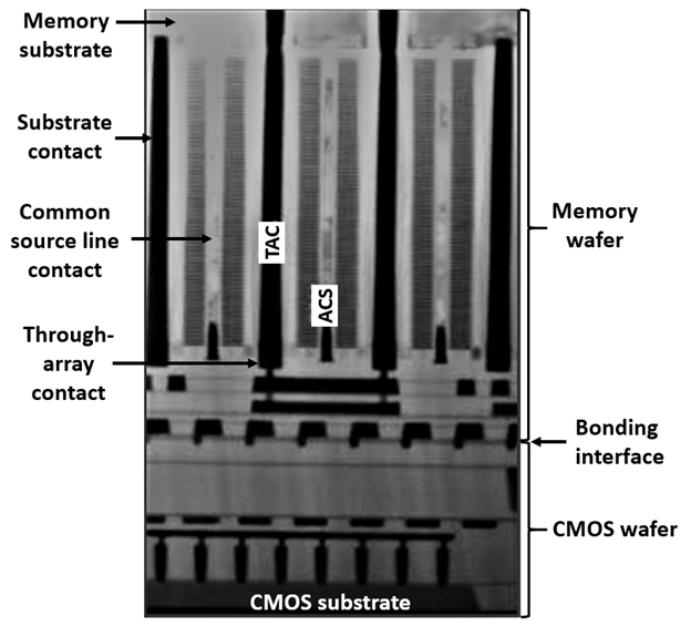
From the image YMTC showed at FMS2018, we can see that the TACs extend from the metal 1 of the memory die up through the array stack and through the substrate silicon (source plate), to connect with the aluminum layer that we saw in the first SEM image, possibly through a re-distribution layer. The CSL contact has been labeled ACS – our guess at this acronym is “array contact slit”.
The TACs are within the memory array or most array edges (just beside the array), so that seems to eliminate the likelihood of TSVs right at the bond pad positions, and they are clearly higher density. Tungsten (W) fills the TSV (or TSC) holes after TSV Si etching and oxide spacer deposition, and then W etch-back followed.
That seems to be about the limit of what we can conclude so far about this part; looking ahead, YMTC announced a 1.33 Tb, 128-layer, quad-level cell part on April 13. Now that YMTC have both TSV and wafer-bonding technologies, in future could we see stacked dies to give us 500- or even 1000-layer devices?
About the authors
Dick James is an almost 50-year veteran of the semiconductor industry, working in the process development, design, manufacturing, packaging and reverse engineering of semiconductor devices. For over 20 years he worked with Chipworks (now part of TechInsights), and is now Fellow Emeritus with TechInsights. He is also a Senior Analyst for TechSearch International, based in Austin, a leading consulting company in the field of advanced semiconductor packaging technology.
Dr. Jeongdong Choe is a Senior Technical Fellow at TechInsights. He holds a Ph.D. in electronic engineering and has over 27 years’ experience in semiconductor process integration for DRAM, (V)NAND, SRAM and logic devices. Dr. Choe’s background includes positions as a Team Lead in R&D for SK-Hynix and Samsung, where he optimized process and device architectures with state-of-the-art technologies for mass production.
References
1. https://www.techinsights.com/blog/ymtc-chinas-first-mass-producer-3d-nand-flash-memory-chips