By Zvi Or-Bach, President & CEO, MonolithIC 3D, Inc.
Shortly after ISSCC 2022, we were intrigued by Alibaba’s presentation of a paper titled “184QPS/W 64Mb/mm2 3D Logic-to-DRAM Hybrid Bonding with Process-Near-Memory Engine for Recommendation. System.” The paper claimed a remarkable improvement of over 1,000 times in AI computing. Promptly, we published a blog about this breakthrough titled “China May Win in AI Computing”. However, we could not find any indication of Alibaba’s revolutionary technology being adopted in the English electronics media until we stumbled upon Techinsights’ advertisements for the Jasminer device teardown. Subsequently, we conducted a follow-up study of Chinese electronics media using Google Translate and uncovered numerous other activities by Chinese semiconductor vendors. It is well-known that the US restrictions on state-of-the-art semiconductor equipment and computing chips have significantly impacted China’s competitive position in the field of AI. Nevertheless, it seems that certain Chinese companies are now exploring alternative approaches, such as Hybrid Bonding, as evidenced by the coverage below.
Let’s start with a bit of a background. In a paper presented at the 2017 IEEE S3S conference, titled “A 1,000x Improvement in Computer Systems by Bridging the Processor-Memory Gap,” we introduced the potential of using hybrid bonding to overcome the “Memory Wall.” We further elaborated on this concept in a book chapter, titled “A 1000× Improvement of the Processor-Memory Gap,” published in the book NANO-CHIPS 2030,published in 2020.
On June 15, 2022, a Chinese article titled “Breakthrough Bypassing the EUV Lithography Machine to Realize the Independent Development of DRAM Chips” reported that Xinmeng Technology had announced the development of a 3D 4F² DRAM architecture based on its HITOC technology. The company claimed that this architecture could be used as an alternative to advanced commercial DRAM. According to the article, this development represents another major innovation breakthrough in the field of heterogeneous integration technology, following the release of SUNRISE, an all-in-one AI chip for storage and computing. The article also reported that Haowei Technology had successfully used Xinmeng’s HITOC technology for the latest tape-out of the Cuckoo 2 chip, resulting in a large-capacity storage-computing integrated 3D architecture.
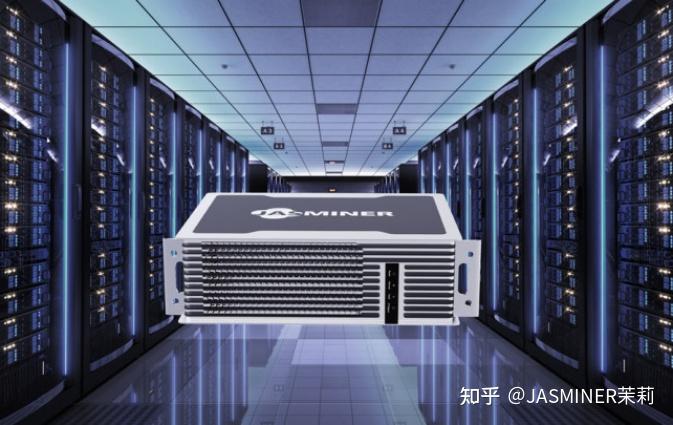
Techinsights is currently promoting a report titled “China breaks through restrictions with advanced chiplet strategy: 3D-IC Breakthrough in Chinese Ethereum Miner.” According to the report, Techinsights discovered a storage mining design in the Jasminer X4 Ethereum miner ASIC, which was developed by the China-based manufacturer Jasminer. The report states that this design is the industry’s first-ever use of DBI hybrid bonding technology with DRAM. Techinsights highlights that the Jasminer X4 demonstrates how a Chinese company can combine mature technologies to creatively produce high-performance, cutting-edge applications even under trade restrictions. The report also reveals that the X4 features a sizable 32 mm × 21 mm logic die that employs the earlier XMC (Wuhan Xinxin Semiconductor Manufacturing Co.) planar 40/45 nm CMOS.

During the 2023 China IC Leaders Summit, Seehi founder Xu Dawen gave a speech entitled “DRAM Storage and Computing Chips: Leading the Revolution of AI Large-Scale Computing Power.” The company has published the speech on its website, and we have selected some of the key statements from it.
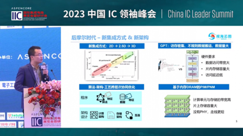

“At present, it is known that a single model requires more than 2,600 servers, which costs about 340 million U.S. dollars when converted into funds, and consumes about 410,000 kWh of electricity per day.” “Different from the model with CNN as the main framework, GPT is characterized by intensive memory access and irregular data handling, and insufficient data multiplexing.”
In his talk Xu referenced the work published by Alibaba at ISSCC2022 – “In 2022, Bodhidharma Academy and Tsinghua Unigroup stacked 25nm DRAM on 55nm logic chips to build neural network computing and matching acceleration in recommendation systems. The system bandwidth reaches 1.38TBps. Compared with the CPU version, the performance is 9 times faster, and the energy efficiency ratio exceeds 300 times.”
During his speech, Xu Dawen presented a table that compared different alternatives to memory cache.
|
Latency (cycle) |
Bandwidth |
|
|
L1 cache |
~3 |
– |
|
L2 cache |
~10 |
TB/s |
|
L3 cache |
~40 |
TB/s |
|
HBM Memory |
~150-300 |
GB/s |
|
Hybrid Bonding 3D memory |
~40-80 |
TB/s |
Table 1: Memory latency and bandwidth comparison.
“Through 3D stacking technology, we can achieve the distance between the processor and DRAM to the micron level or even sub-micron level. In this case, the wiring is very short and the delay is relatively small. Through this technology, thousands or even hundreds of thousands of interconnection lines can be completed per square millimeter, achieving higher bandwidth. In addition, eliminating the PHY and shorter wiring will result in lower power consumption and better cost performance. The entire chip is composed of multiple tiles, and each tile is stacked by DRAM and logic. The DRAM part is mainly to provide high storage capacity and high transmission bandwidth, and the logic part is mainly to do high computing power and efficient interconnection. The NoC communicates between the tiles. This NoC is an in/through NoC design. It is interconnected with adjacent tiles on the same plane and communicates with the memory in the vertical direction.”
Finally he referenced their device called SH9000 GPT “which is based on the customer’s algorithm and is integrated around the architecture layer, circuit layer, and transistor layer across layers. This set of technologies has successfully achieved excellent cost and energy efficiency ratios on mining machine chips. The theoretical peak power consumption of the SH9000 chip design may be slightly lower than that of the A100 (Nvidia), and the actual RTOPS is expected to be twice that of the opponent, which can achieve a better energy efficiency ratio.”
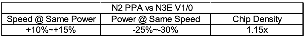
Considering that both logic and DRAM devices were manufactured in China using relatively “old” nodes and still perform competitively compared to TSMC’ state-of-the-art devices and systems, it should be a matter of concern for all of us. This is particularly true since improvements solely through node scaling are no longer as significant as they used to be. The following table, released by TSMC for their 2025 N2 node, illustrates this point.

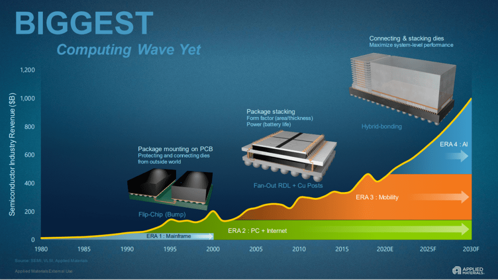
Undoubtedly, the US restrictions on state-of-the-art semiconductor equipment and computing chips have greatly impacted China’s competitive position in the field of AI. However, it appears that some Chinese companies are now exploring alternative approaches, such as Hybrid Bonding and heterogeneous system integration. While this new path presents its own challenges, it offers unprecedented advantages. Delaying the adoption of this new approach could result in an insurmountable gap in the future. The following chart from Applied Materials illustrates this point clearly.