BY TOM ADAMS, consultant, Nordson SONOSCAN, Elk Grove Village, IL
X-ray and ultrasound are both well known for being able to image internal features, including structural defects, in solid objects without damaging or destroying those objects. The two technologies are also known for being complementary to each other: an internal structure of a certain type in a certain material that cannot be imaged satisfactorily by one of the technologies can very often be imaged by the other.
Some basics: X-rays are part of the electro-magnetic spectrum, and have shorter wavelengths than visible light, though not as short as gamma rays. Shorter wavelength means higher frequency and higher energy. X-rays are not reflected from the surfaces of solid materials except at very low oblique incident angles, and although there are some industrial applications for reflective X-ray, it is not generally available commercially. Ultrasound and X-ray are both attenuated – but to different degrees – by the material they are passing through. X-ray images display internal structure by displaying local differences in the brightness of the arriving beam (absorption contrast imaging). In an X-ray system, varying the voltage controls the penetration into the material. Spatial resolution is very high: X-ray can resolve single features into the submicron range although final resolution depends on the detector and the focus of the X-ray source.

Ultrasound is mechanical energy, and not part of the electromagnetic spectrum. It travels far more slowly than X-ray through solid materials, moving at speeds ranging from a few thousand meters per second up to 18,000 meters per second (diamond). Ultrasonic imaging frequencies for industrial applications range from about 5 MHz to about 400 MHz. Penetration into a given material depends on the material’s elastic properties. Because of high attenuation, a highly elastic material such as rubber can be imaged only at very low frequencies – a few MHz or less, depending on the sample thickness. But low-attenuation materials such as silicon and diamond can use 400 MHz. Most applications in the electronics industry use frequencies between 30 and 230 MHz. Ultrasound is reflected by all interfaces between materials, and is partially transmitted through many of those interfaces. Unlike X-ray, it will not travel through air; a solid-to-air interface causes near 100 percent reflection.
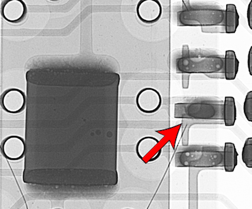
The X-ray image of one of the eight devices in a memory strip is shown in Figure 1. The strip was imaged by a Nordson DAGE QuadraTM 7 system to identify internal defects that might cause electrical failures during service. Figure 1 reveals all features from the top of the device’s plastic package to the bottom of the board below. The circular features are holes in the board, and the pale gray horizontal/diagonal lines are traces on the board. Voltage was 110 Kv, and power was 7 watts. A sharpening filter and a contrast filter were both applied.

The large vertical gray feature is the plastic package. The silicon die within the package is not visible because it attenuates the X-ray beam very slightly, but its position may be deduced from the wires leading into the package. The darker rectangle in the lower half of the die area is a capacitor on the other side of the board.
There are no broken wires or other obvious defects here, but there is an oval area in one lead’s bond to a pad at right, marked in Fig. 1 by an arrow. It is somewhat darker than the other bonds.
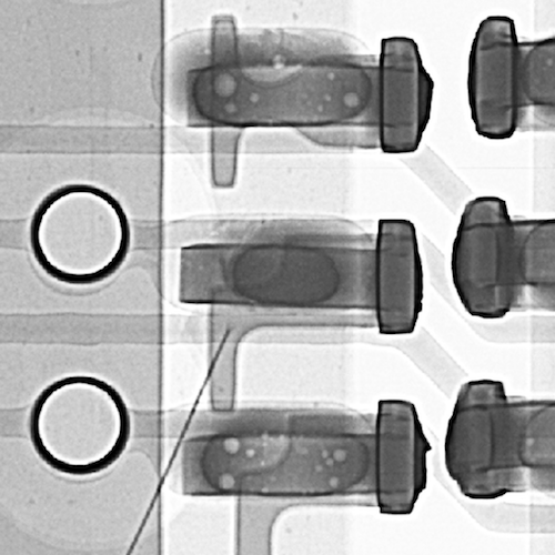
This feature is shown at higher magnification at the center of Figure 2. The dark oval blob at the center of the joint is the solder, which has failed to spread out and wet the two surfaces (the lead from the die and the bond pad on the PC). Its greater thickness relative to the solder in surrounding joints makes it more attenuating and therefore darker. But the lack of wetting means that the connection between the lead and the pad is poor or nonexistent.
On the pad below this one the solder has wetted most of the desired contact area – note the larger, more transmissive oval. In the process, it has picked up a few air bubbles. Bonding is not likely to be compromised unless the air bubbles comprise 40 per cent or more of the desired soldier volume. Other nearby joints have wetted their joints, and some also have air bubbles.
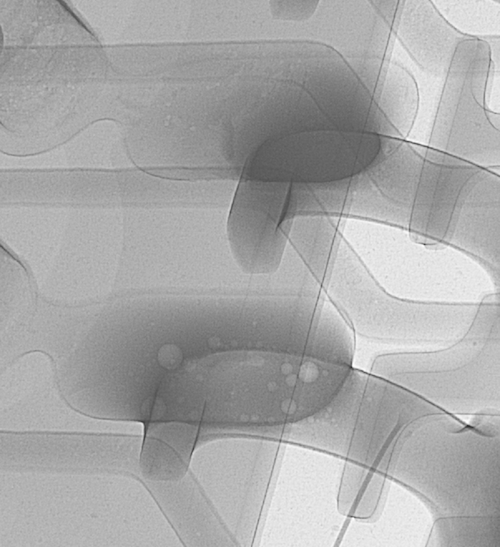
The same features can be seen by imaging the component at an angle, as seen in Figure 3. The local distance through a feature is more varied when viewing at an angle. The unbonded joint at top is an oval of varying darkness, although the voids in the lower joint are nicely visible.

The same memory strip was next imaged by a Nordson SONOSCAN C-SAM® tool using the C-mode imaging technique. A transducer of 120 MHz was used. Return echoes from each pulse were gated on a depth from just below the top surface of the plastic package to the bottom of the die. A gate is the defined depth range from which echoes returned from material interfaces are used making the acoustic image. Echoes from below or above this depth are ignored. Gating thus limits view thickness and avoids confusion in identifying the depth of a particular feature.
The memory strip is shown acoustically in Figure 4. Because the top surface of the package and the die attach are excluded from the gate, the only expected echo within the gate is from the interface between the mold compound and the die face. In seven of the devices, this interface appears gray, indicating that echoes of modest amplitude were reflected from the interface between the two solid materials. The gray areas are somewhat mottled, perhaps due to inhomogeneities in the mold compound.

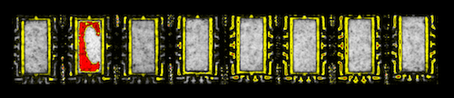
But in the image of the second device (Figure 5) most of the die area is red, indicating near-total ref lection of the arriving pulse. When pseudocolor is used to identify features, red is often selected to identify the interface between a solid material and a gas, typically air. What has happened here is that the mold compound is delaminated from the die face over much of the area of the die, leaving a thin air gap. In the original monochrome image, this region would be bright white, while regions reflecting no ultrasound would be black, and interfaces between two solids would be some shade of gray.

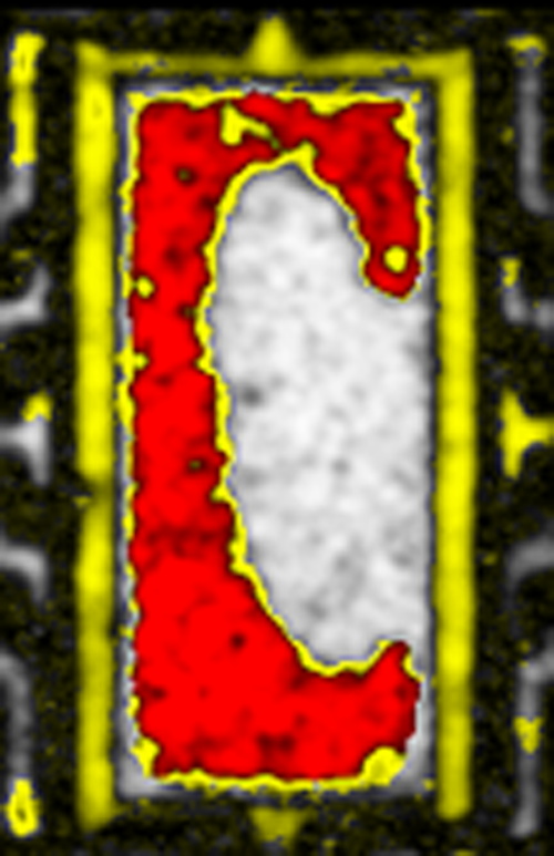
Even a small die face delamination may expand during service and lift wires from their bonds, causing electrical failure. A large-area delamination such as this one could also cause the die to overheat and fail, depending on the intended power dissipation of the device.
The memory strip was next imaged by a method that produces a nonde- structive cross-section through the sample being imaged. The method is known as Q-BAMTM (for Quantitative B-scan Analysis Mode), and produces a cross-sectional image through a selected vertical plane that is dimensionally the same as an optical photo of destructive sectioning through the same vertical plane.
To make the Q-BAM image, the sample is first imaged by the C-mode method in order to select the vertical plane through which nondestructive imaging will be performed. Figure 4 is therefore repeated in the lower part of Figure 6. The white line running horizontally through the memory strip defines the vertical plane through which the memory strip was nondestructively sectioned.
The nondestructive image in the top part of Figure 6 was created by scanning a sequence of very thin gates. On the first pass along the white line, the transducer accepted for imaging only echoes that originated in a very thin gate at the very bottom of the depth of interest. The transducer then moved to the next gate above, and scanned back across the sample. Back- and-forth scanning of gates continued until the surface was reached and the nondestructive cross section was complete.
The cross section is the top portion of Figure 6. The scale at upper left divides the vertical extent of the cross section into ten segments. The bold red features just above and below the top of the mold compound are simply echoes from the water-to-mold compound interface. The very numerous small features that give the impression of raining down from the surface are simply inhomogeneities in the mold compound, and not voids or other defects.

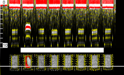
The Q-BAM image reveals that the device having the red delamination in the C-mode view in the Q-BAM image is strongly arched: the domed profile would look just as domed in an optical image if the device were physically sectioned. In the C-mode view below, notice where the white line passes through this device: the entire width of the die is delaminated here, but if the white line had been drawn a bit higher the red delamination at that location would have been much narrower.
The remaining seven devices show some dimensional variation when viewed in cross section. The second device from the right end is visibly tilted, perhaps enough to stress or break wires.
There are other capabilities in which the two technologies possess useful differences. Ultrasound can measure the depth of an internal feature directly by measuring the transit time of the reflected echo. If the sample can be turned on its side for imaging, the depth of a feature seen from above can be measured directly.
X-ray can increase image penetration by raising the voltage. Ultrasound can increase penetration to some extent by lowering the frequency, but in both X-ray and ultrasound brightness is controlled only after the image is made.
Striking an air-filled gap, ultrasound is almost entirely reflected as a very strong echo, even if the gap of sub- micron thickness. X-ray is not reflected at all, but will image a gap thick enough to cause detectable attenuation.
Both technologies can produce 3D images. X-ray (Nordson DAGE X-Plane® system) collects a full data set from many different angles and uses software to create the image. Ultra- sound performs planar scanning at a number of thin gates and creates the 3D image from this data.
Because it is not reflected by surfaces, X-ray can produce angled internal views such as Figure 3. Simply by using a very wide gate (e.g., nearly the entire thickness of a component) ultrasound can produce a single planar view showing internal features at multiple depths, but some features may block deeper features. Ultrasound can also produce individual images of multiple gates during the same scan.
There are several other paired capa- bilities, but the value of applying both technologies to a problem is very direct: internal structural anomalies have nowhere to hide.
C-SAM® is a registered trademark of Nordson SONOSCAN.