Synopsys, Inc. today announced a collaboration with TSMC to develop a broad portfolio of DesignWare interface IP, logic libraries, embedded memories, and one-time programmable (OTP) non-volatile memory (NVM) IP on TSMC’s 5-nanometer (nm) FinFET Plus (N5P) Process. This collaboration reinforces the longstanding relationship between the two companies to provide designers with the high-quality IP needed to lower risk, differentiate their system-on-chips (SoCs), and accelerate their time-to-market.
Seoul Semiconductor Successfully Obtains Permanent Injunction against Patent Infringement in U.S. Following German Court’s Injunction Orders
Seoul Semiconductor Co., Ltd. (KOSDAQ 046890) (“Seoul”), a global innovator of LED products and technology, announced on September 26 that it won a patent infringement lawsuit against Service Lighting And Electrical Supplies, Inc., an operator of “1000bulbs.com” – the largest online light bulb distribution channel. The Texas Northern District federal court issued a permanent injunction against the sales of more than 50 lighting products, as well as any colorable variations of those products unless they have been licensed, according to the parties’ stipulation.
Toshiba Memory America Introduces Next-Gen Serial Interface NAND
Toshiba Memory America, Inc. (TMA), the U.S.-based subsidiary of Toshiba Memory Corporation, today announced the launch of a new family of SLC NAND flash memory products for embedded applications. Compatible with the widely used Serial Peripheral Interface (SPI), Toshiba Memory’s second-generation Serial Interface NAND can be used in a wide range of consumer and industrial applications that require high-speed data transfers, including flat screen TVs, printers, wearable devices, and robots.
Researchers Report a New Way to Produce Curvy Electronics
Contact lenses that can monitor your health as well as correct your eyesight aren’t science fiction, but an efficient manufacturing method – finding a way to produce the curved lenses with embedded electronics – has remained elusive. Until now. A team of researchers from the University of Houston and the University of Colorado Boulder has reported developing a new manufacturing method, known as conformal additive stamp printing, or CAS printing, to produce the lenses, solar cells and other three-dimensional curvy electronics.
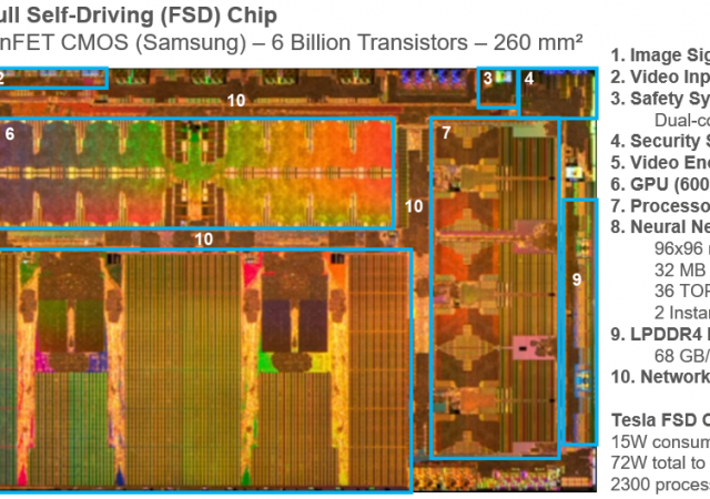
A Deep Dive into AI Chip Arithmetic Engines
Tesla’s autopilot chip executes 72-trillion additions and multiplications per second: It better get the math right
Development of Highly Sensitive Diode, Converts Microwaves to Electricity
The Japan Science and Technology Agency (JST), Fujitsu Limited, and the Tokyo Metropolitan University announced that they developed a highly sensitive rectifying element in the form of a nanowire backward diode, which can convert low-power microwaves into electricity. Through JST’s Strategic Basic Research Programs, the technology was developed by researchers led by Kenichi Kawaguchi of Fujitsu Limited and Professor Michihiko Suhara of the Tokyo Metropolitan University.
Achronix Joins TSMC IP Alliance Program
Achronix Semiconductor Corporation, a provider in FPGA-based hardware accelerator devices and high-performance eFPGA IP, has joined the TSMC IP Alliance Program, a key component of TSMC Open Innovation Platform® (OIP). Achronix’s award-winning Speedcore eFPGA IP is optimized for high-end and high-performance applications. Speedcore eFPGA IP is available today on TSMC 16nm FinFET Plus (16FF+) and N7 process technologies, and it will be soon available on TSMC 12nm FinFET Compact Technology (12FFC).
Samsung Introduces Industry’s First 0.7μm-pixel Mobile Image Sensor
Samsung Electronics Co., Ltd. today introduced the industry’s first 0.7-micrometer (μm)-pixel image sensor, the 43.7-megapixel (Mp) Samsung ISOCELL Slim GH1. Thanks to advanced ISOELL Plus technology, the new ultra-high-resolution GH1 image sensor embraces 43.7-million 0.7μm-sized pixels in a super-small package, providing the optimum solution for slim full-display devices.
UMC Receives Final Approval for 100% Acquisition of Mie Fujitsu Semiconductor
United Microelectronics Corporation (NYSE: UMC; TWSE: 2303) (“UMC”), a global semiconductor foundry, today announced that the company has satisfied all closing conditions, including final approval from all relevant government agencies, for the full acquisition of Mie Fujitsu Semiconductor Limited (MIFS), the former 300mm wafer foundry joint venture between UMC and Fujitsu Semiconductor Limited (FSL). The completion of the acquisition is scheduled for October 1, 2019.
Bottom-Up Synthesis of Crystalline 2D Polymers
Scientists at the Center for Advancing Electronics Dresden (cfaed) at TU Dresden have succeeded in synthesizing sheet-like 2D polymers by a bottom-up process for the first time. A novel synthetic reaction route was developed for this purpose. The 2D polymers consist of only a few single atomic layers and, due to their very special properties, are a promising material for use in electronic components and systems of a new generation. The research result is a collaborative work of several groups at TU Dresden and Ulm University and was published this week in two related articles in the scientific journals “Nature Chemistry” and “Nature Communications”.