A nanoscale gold butterfly provides a more precise route for growing/synthesizing nanosized semiconductors that can be used in nano-lasers and other applications. Hokkaido University researchers have devised a unique approach for making nanosized semiconductors on a metal surface. The details of the method were reported in the journal Nano Letters and could further research into the fabrication of nanosized light and energy emitters.
MEMS-FHE Device Integration Gets Real
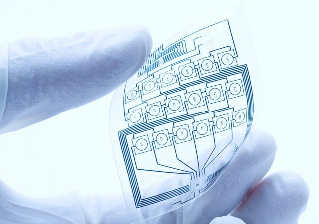
MEMS technology has changed human interaction with electronic devices. Introduced in the 1990s, the first mass-market MEMS devices were used for inkjet printheads and automotive airbag crash sensors. Today, MEMS are ubiquitous, with billions of the tiny devices adding intelligence and interactivity to smartphones, smart speakers, wearables, automobiles, biomedical devices, remote monitoring and event detection systems, and countless other applications. Integrating MEMS with Flexible Hybrid Electronics (FHE) is an important step in the evolution of this miniaturized intelligent sensing technology, paving the way for its use in new classes of flexible, conformal devices.
Flexible Hybrid Electronics Comes to Bio-Interfacing and Biodegradable Electronics at FLEX|MSTC 2020
VTT Technical Research Centre of Finland Ltd (VTT) has its sights set high.
Xperi Enters into New Patent and Technology License Agreement with SK hynix
Xperi Corporation (NASDAQ: XPER) (“Xperi”) today announced that it entered into a new patent and technology license agreement with SK hynix, one of the world’s largest semiconductor manufacturers. The agreement includes access to Xperi’s broad portfolio of semiconductor intellectual property (IP) and a technology transfer of Invensas DBI Ultra 3D interconnect technology focused on next-generation memory.