FAVIER SHOO, Yole Développement, Singapore
In 2018, 75% of Fan-Out Packaging capital expenditure (CapEx) was invested by the top three manufacturers in this area: Taiwan Semiconductor Manufacturing Company (TSMC), Samsung Electronics and Powertech Technology Inc. (PTI). TSMC is a foundry, Samsung Electronics is an integrated device manufacturer (IDM) and PTI is an outsourced assembly and test (OSAT) company. These players all come from different business models, yet they are engaged in the same technology, with different Fan-Out Packaging solutions and strategies. This has resulted not only in an increasingly divided market, between high-end and low-end applications of Fan-Out Packaging, but also an unavoidable cost vs. performance battle between panel-level and wafer-level processing.
Fan-Out Packaging market value is expected to grow at a 19% compound annual growth rate (CAGR) from 2019-2024, reaching $3.8B. Most industry players remain positive about the growth of Fan-Out Packaging, anticipating a surge in productivity from current levels. For instance, increased CapEx and R&D spending will enable new Fan-Out Packaging adoption in 5G and High Performance Computing (HPC) applications. Suppliers are heavily reliant on these few key manufacturers to fuel the strong growth in Fan-Out Packaging. They are all expected to power forward with more breakthroughs. Also, Chinese OSATs are well-positioned to invest progressively in Fan-Out Packaging.
Equipment and materials market revenue forecast
Although Fan-Out (FO) Packaging is still a relatively small market amongst other popular packaging platforms, it can cover high-end High-Density (HD) FO and low-end Core FO applications. Historically, FO Packaging is essential to applications such as Power Management Integrated Circuits (PMICs), Radio-Frequency (RF) Transceivers, Connectivity Modules, Audio/Codec Modules and Radar Modules and Sensors. It was, however, the adoption by Apple’s Application Processor Engine (APE) of TSMC’s integrated FO Package-on-Package (inFO-PoP) platform that started to fuel its popularity and made HD FO possible. Now, there is no doubt the industry is no longer as overexcited about FO packaging as it was during the TSMC/Apple buzz. However, in HD FO, TSMC is the sole leader, and is not only using inFO for APE. It is also extending it into new exciting technologies like inFO-Antenna-in-Package (AiP) for fifth-generation (5G) wireless communication, and inFO-on-Substrate (oS) for HPC. So, FO Packaging is still maintaining its centrality as a popular option for mega-trend driven applications like AiP, HPC and Systems-in-Packages (SiPs). FO Wafer Level Packaging (WLP) capacity expansion is therefore expected moving forward. Samsung Electro-Mechanics (SEMCO) and PTI have been catching up aggressively, with a different strategy, since 2016. A new milestone was achieved by SEMCO in 2018, with the latest release of a FO Panel-Level Packaging (PLP) APE-PMIC in the Samsung Galaxy Smartwatch. Also, PTI had gone into FOPLP production for MediaTek’s PMIC and Audio Transceiver. Moving forward, investments by manufacturers will be modest in the short term and strong in the long term. Regardless, a new high volume application is anticipated to fuel further tremendous growth in the FO Packaging market space.
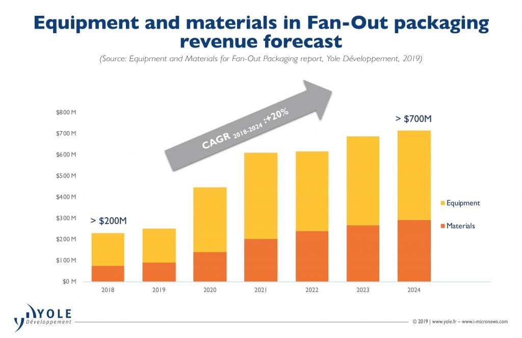
Based on new sales, made from incremental production volumes, the equipment and materials revenue for FO packaging is expected to grow from over $200M in 2018 to over $700M in 2024 at more than 20% CAGR (Figure 1). With production players slashing growth projections in 2019, suppliers of FO Packaging are now anticipating a smaller CapEx in 2019. Nevertheless, Equipment and Materials suppliers are well-positioned in the FO Packaging supply chain to gain business from long-term growth. Megatrend-driven demands, in the long run, are expected to provide the impetus to push for an uptick in Equipment and Materials revenue from FO Packaging eventually.

FOPLP vs FOWLP unfolds
FO Packaging suppliers are grappling with two conflicting motivations of cost reduction and Return-on-Investment (ROI) justification. FOWLP suppliers are worried about a cost-price war if FOPLP is adopted and finally overloads the market with supply. There will continue to be pressure to make a strategic decision to invest in either FOWLP or FOPLP because core FOWLP capacity is showing signs of under-utilization. Coupled with FOPLP penetration, the over-supply risk is increasingly being recognized. Yet, there are strong motivations to venture into FOPLP because end-customers are demanding lower-cost FO Packages. As such, some FO Packaging suppliers are sitting on the fence. In this divided environment, they would rather gain less business with certainty than embrace uncertainty that could involve losing on larger investments.
FOWLP suppliers are unable to stop the penetration of FOPLP suppliers despite the volume of FO being relatively small compared to the huge volume of Printed Circuit Boards sold, which enables panel-level manufacturing. This forces FOWLP suppliers to focus on higher-end challenges that FOPLP cannot achieve technically in the near term. For example, TSMC’s supply chain is expected to grow because of the extension of HD FO applications.
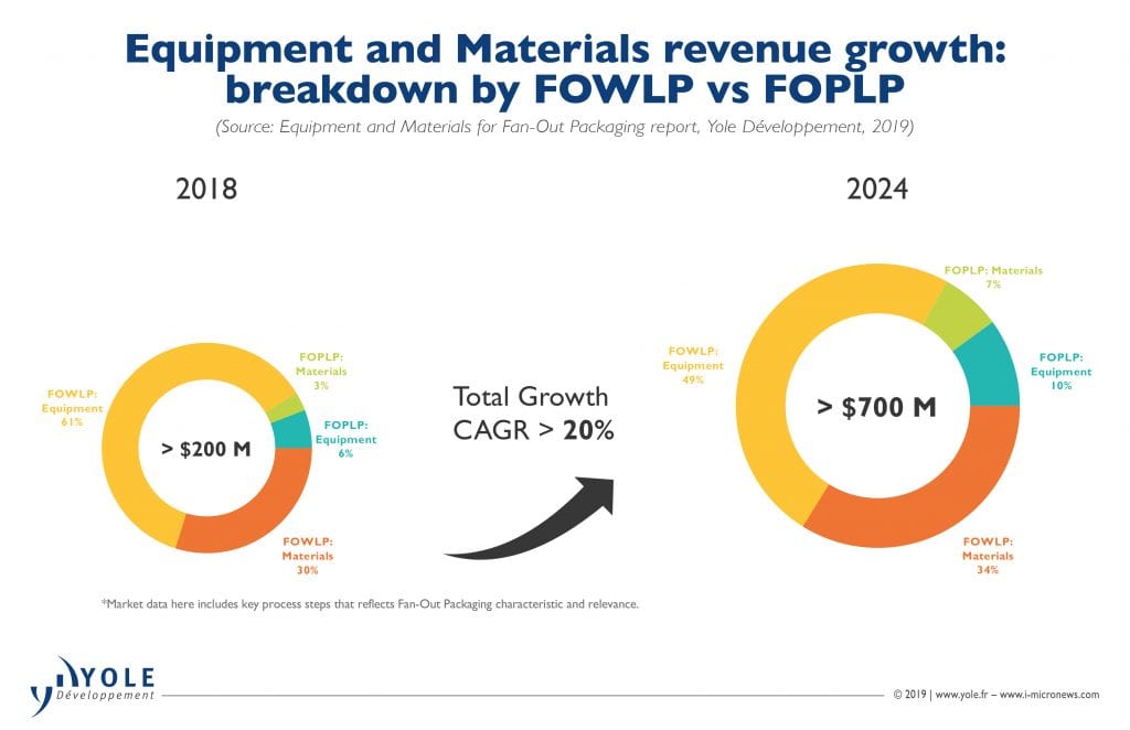
A lower production penetration rate of FOPLP is expected in 2019 even though more players are involved compared to 2018. In 2019, FOPLP suppliers are expected to expand slowly, with more players adopting panel capabilities. Presently, the volume is not big enough to justify further investment in panel production, especially when core FO is already experiencing under-utilization. However, in the long run, the expansion of FOPLP is expected to increase because new players are driving a low-cost proposition into the FO packaging market. Also, it has been proven technically feasible by SEMCO and PTI. FOWLP equipment’s share of the FO equipment and materials market is projected to drop by 12% from 2018 to 2024. On the other hand, FOWLP materials, FOPLP equipment and FOPLP materials’ shares are all expected to grow by 4% each (Figure 2).
Activities of key Fan-Out packaging manufacturers
For commercialization of FOWLP packages, the established OSATs are Advanced Semiconductor Engineering (ASE), Amkor Portugal, formerly Nanium, the Jiangsu Changjiang Electronics Technology (JCET), which includes STATS ChipPAC and Jiangyin Changdian Advanced Packaging (JCAP), Deca and Nepes. OSATs who pursue FO packaging capabilities include Amkor Korea, ASE, Deca, Huatian, and Siliconware Precision Industries Ltd (SPIL). More OSATs are becoming involved in FOWLP; they are the main contributors for core FO and are all targeting volume production, though they are at different levels of development status.
The FOWLP supply chain is simpler and controlled by experienced players in the semiconductor industry, but it requires collaboration at the design level, in contrast to flip-chip ball grid array (FCBGA). FOWLP involves simplification and consolidation of the packaging, assembly and testing in mid-range infrastructure, where the cost of production is essentially in the wafer fab. FCBGA needs a substrate supplier, and wafer fab capacity for redistribution layers (RDLs), wafer bumps, and assembly and testing. In comparison, FOWLP only needs assembly, wafer fabs for RDLs and wafer bumps and testing. There is therefore a shift in value chain created by FOWLP.
TSMC has been the sole contributor to HD FO since 2016 and has adopted a unique strategy (Figure 3). It is not only an advanced foundry for the front-end (FE) but also a high-end packaging house for the back-end (BE). This business model will continue to lead the way to create new value and breakthroughs. With TSMC’s InFO being able to package high-end APEs for Apple’s iPhone, a new market, HDFO, was generated. InFO-oS technology is now being utilized for HPC in Low Volume Manufacturing (LVM). Also, InFO-MS (Memory on Substrate) has been developed for servers and InFO-AiP for 5G.
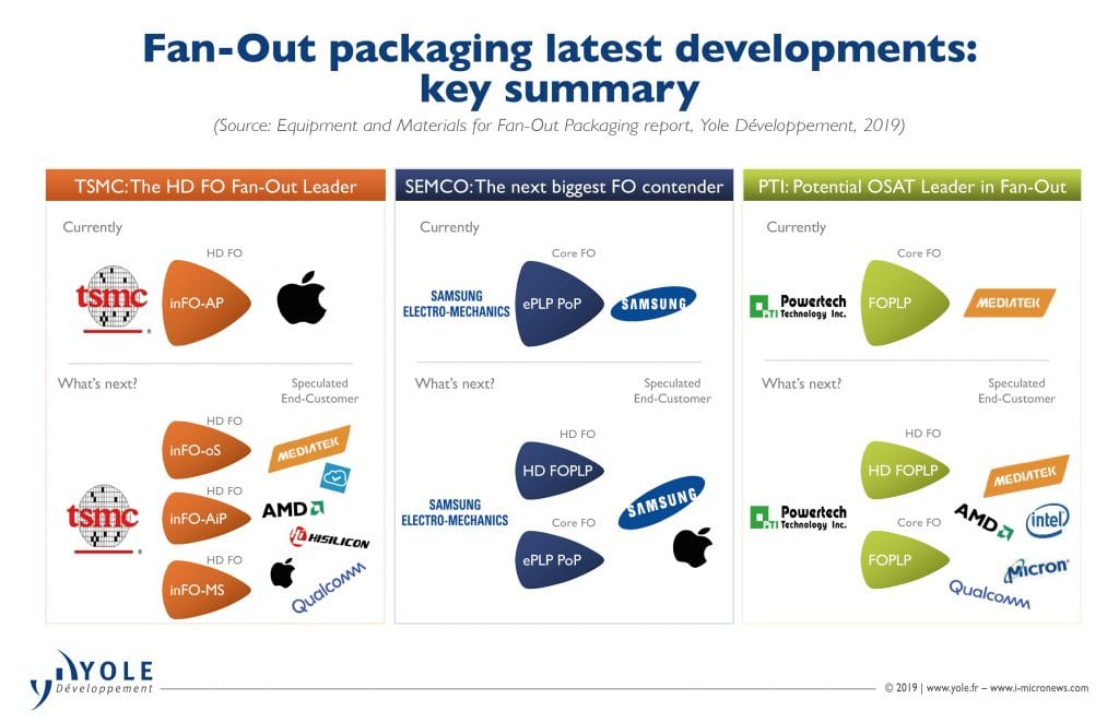
SEMCO is the next biggest FO contender, being part of Samsung Electronics, which is an IDM. Samsung has been instrumental in design, memory, logic, packaging, chipset assembly and end-product and can, therefore, drive breakthroughs internally. SEMCO, being part of the Samsung group, is pressured to develop differentiated yet cost-effective technology. In 2018, SEMCO achieved a new milestone by rolling out APE-PMIC devices with FO embedded panel-level packaging (ePLP) PoP technology for the Samsung Galaxy Watch. SEMCO will continue to innovate for a cost-effective HDFO market space in order to compete with TSMC for Apple’s packaging and FE business again. In years to come, SEMCO’s HDFO is expected to be utilized first in Samsung’s smartphones. Besides, a reorganization between SEMCO and Samsung Electronics could be beneficial for Samsung’s position as a full turnkey provider for a FE+BE bundle. This will be a direct battle against TSMC fighting to be the supplier for Apple’s APE die and packaging business.
Currently, PTI has successfully secured MediaTek’s business in automotive radar applications. Qualcomm and MediaTek will continue to request mid-end to high-end devices at a lower price from OSATs. With new megatrend applications requesting more functionalities and shorter routing paths, a larger package with multiple dies, like a processor-memory combination, is ideal. PTI is a good choice for fabless companies, IDMs and foundries because it is already a specialist in memory packaging and a driver of FOPLP. PTI is investing $1.6B in a new FOPLP fab and we can expect it to emerge as a cost-effective leader in FOPLP technology in the years to come for core FO.
Technology evolution
Fan-out packaging technology (Figure 4) is not only a bridge to resolve chip-package interaction (CPI) mismatch in pitch size; It is also a viable solution for heterogeneous integration of functionality in a desired package dimension and design, potentially for mm-wave 5G and cloud data server applications.
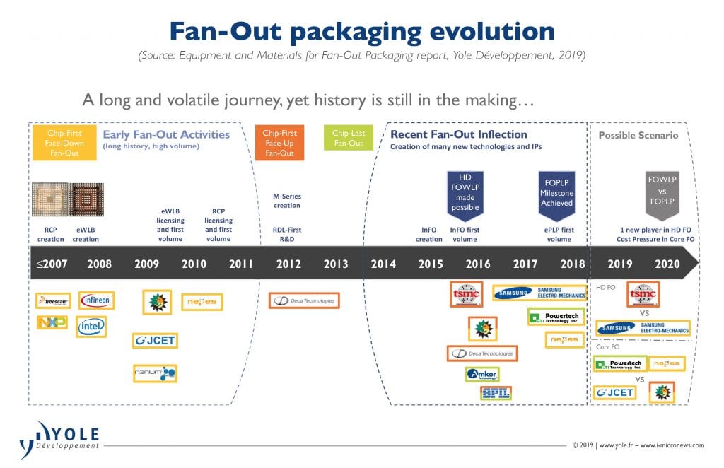
Chip-first fan-out solutions are still well-established in the market. Since 2009, Embedded Wafer Level Ball Grid Array (eWLB) has been the most famous FO technology in the core market. Its long history and device-proven qualification have provided customers with confidence and it is therefore continually being adopted. It is considered a mature process for single-die packaging and potentially a good solution for system-in-package (SiP) manufacturing, with products that embed several active dies and numerous passives already available.
As there are several licensees, multi-sourcing is possible. This is key for supplying end-customers, especially for those with high-volume needs, such as the cellphone market. Redistributed chip packaging (RCP) technology has better performance in terms of die shift, and consequently easier photolithography steps, as well as better resolution. However, it has suffered from a lack of licensees and cost competitiveness compared to eWLB. Although it had some success thanks to the NXP portfolio, it is progressively disappearing.
TSMC has maintained technology leadership in HDFO and extended it even further with high-volume manufacturing (HVM) InFO package-on-package (InFO-PoP) for Apple’s latest APEs. In addition, TSMC is rolling out InFO on substrate (InFO-oS) for high-performance devices in HPC applications. Fan-out antenna-in-package (FO-AiP) has gained the interest of FO players because FO has well-known capabilities in radar. With FO packaging, the embedded RF chip will suffer less interference. In this manner, extra performance value can be generated for FO-AiP. Also, FO packaging can adopt memory-on-substrate at TSMC and potentially PTI. This will become an alternative to 2.5D interposers. The key technical benefit of FOWLP is the ability to integrate dies together flexibly while remaining thin. It can displace 2.5D interposers with fine line/space (L/S) FO packaging capabilities on substrates. It can also displace flip chip and advanced substrate processes.
PLP must create a new production infrastructure, as front-end equipment cannot be reused for this purpose. PLP can leverage WLP knowledge and infrastructure and use it on printed circuit board/flat-panel display (FPD)/photovoltaic industry equipment. This is not simple, as it needs some reengineering, but it is happening.
About the author
Favier Shoo is a Technology and Market Analyst in the Semiconductor & Software division at Yole Développement, part of Yole Group of Companies. Based in Singapore, Favier is engaged in the development of technology & market reports as well as the production of custom consulting reports.
Editors’ Note: This article originally appeared in the October 2019 issue of Semiconductor Digest.