Plessey, an embedded technologies developer at the forefront of microLED technology for the augmented reality (AR) and mixed reality (MR) display market, announced today at Photonics West its’ partnership with WaveOptics, the leading designer and manufacturer of diffractive waveguides.
Update: TSMC’s 5nm CMOS Technology Platform
At the International Electron Devices Meeting (IEDM) in San Francisco December 7-11, Geoffrey Yeap presented the talk “5nm CMOS Production Technology Platform Featuring Full-Fledged EUV and High-Mobility Channel FinFETs with Densest 0.021µm2 SRAM Cells for Mobile SoC and High-Performance Computing Applications”. Contributing Editor Dick James provides an update on his original pre-IEDM blog.
2019 Global Silicon Shipments Dip From 2018 Record High But Revenue Remained Stable Above $11 Billion
Worldwide silicon wafer area shipments in 2019 declined 7 percent from the 2018 record high while revenue remained above the $11 billion mark despite a global silicon revenue slip of 2 percent over the same period, the SEMI Silicon Manufacturers Group (SMG) reported in its year-end analysis of the silicon wafer industry. Silicon wafer area shipments in 2019 totaled 11,810 million square inches (MSI), while the industry logged shipments of 12,732 million square inches in 2018. Revenues in 2019 totaled $11.15 billion, edging down from the $11.38 billion posted in 2018.
CEA-Leti Develops Tiny Photoacoustic-Spectroscopy System For Detecting Chemicals & Gases
Leti, an institute of CEA-Tech, has developed a photoacoustic spectroscopy technology for monitoring dangerous chemical emissions and traces of gas that could reduce the cost and the size these systems by a factor of 10 or more compared to existing tools. To be presented in an invited paper at Photonics West 2020 titled “Micro PA detector: pushing the limits of mid-IR photoacoustic spectroscopy integrated on silicon”, the detector also provides high immunity to external noise and high sensitivity and selectivity.
ZEISS Accelerates Semiconductor Package Failure Analysis by Orders of Magnitude with Crossbeam Laser FIB-SEM
ZEISS today introduced the ZEISS Crossbeam Laser — a new family of site-specific focused ion beam scanning electron microscope (FIB-SEM) solutions that accelerate package failure analysis and process optimization for advanced semiconductor packages. Integrating a femtosecond laser for speed, a gallium ion (Ga+) beam for accuracy, and SEM for nanoscale-resolution imaging, the ZEISS Crossbeam Laser family provides package engineers and failure analysts with the fastest cross-section solution at the highest imaging performance, while providing minimal sample damage.
SEMI Postpones SEMICON China, Suspends SEMICON Korea in Response to Coronavirus Outbreak
In accordance with government guidelines and to protect the health and safety of exhibitors and guests, SEMI announced Tuesday the postponement of SEMICON/FPD China 2020 and related events originally scheduled for March 18-20, 2020. SEMI China is actively working on a contingency plan for rescheduling of the event and will keep you informed as soon as a confirmed plan is in place.
NeoPhotonics Samples High Power Semiconductor Optical Amplifiers and Narrow Linewidth Lasers for Coherent Lidar Transceivers
NeoPhotonics Corporation (NYSE: NPTN), a leading designer and manufacturer of advanced hybrid photonic integrated circuit based modules and subsystems for bandwidth-intensive, high speed communications networks, today announced that it is sampling high power Semiconductor Optical Amplifiers (SOAs) and Narrow Linewidth (NLW) Distributed Feedback Lasers (DFB) lasers for long range automotive Lidar (“light detection and ranging”) applications.
ON Semiconductor to Explore Sale of Manufacturing Facility in Belgium
ON Semiconductor Corporation (Nasdaq: ON), driving energy efficient innovations, today announced it is exploring a sale of its manufacturing facility in Oudenaarde, Belgium. The company will begin searching for strategic partners that are willing to enter into a mutually beneficial arrangement that the company expects will facilitate an orderly transition of products from its Oudenaarde facility to other facilities within the ON Semiconductor network.
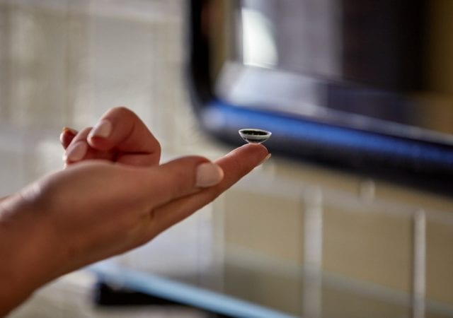
Next Generation of Mobile Devices Will Be Invisible
SEMI’s Nishita Rao caught up with Mike Wiemer, Ph.D., VP of Engineering, CTO and co-founder, Mojo Vision, to preview his February 25 keynote, The Art of the Possible, at FLEX|MEMS & Sensors Technical Congress (MSTC) 2020, February 24-27 at the DoubleTree by Hilton in San Jose, California.
SEMI-FlexTech Launches Six New Projects to Accelerate Flexible Hybrid Electronics Innovation
SEMI-FlexTech today announced the launch of six projects to accelerate sensor and sensor system innovations for new applications in industries including healthcare, automotive, industrial and defense. In collaboration with the U.S. Army Research Laboratory (ARL), FlexTech, a SEMI Strategic Association Partner, will provide more than $2.3 million in funding for the projects aimed at maturing the flexible-hybrid electronics (FHE) technology ecosystem