By HYO SEON SUH, senior researcher, ANNELIES DELABIE, principal member of technical staff , and SILVIA ARMINI, principal member of technical staff at imec, Leuven, Belgium.
Photolithography is one of the cornerstone technologies that has enabled the continuous downscaling of micro- and nanoelectronic devices over the last half century. This process uses light to transfer a pattern from a photomask to a photoresist material on the substrate. A series of chemical treatments then either etches the exposed pattern onto the substrate or enables the deposition of a new material in the desired pattern.
With further downscaling, this conventional top-down patterning transfer process is becoming increasingly complicated and expensive. The further miniaturization of devices requires the patterning of features with critical dimensions below 20nm. In addition to scaling the resolution, the accurate pattern placement is becoming very challenging. The reduction of the active footprint also comes with the advent of 3D structures, with high aspect ratios and complex shapes.
About five years ago, the industry began to take an interest in alternative patterning approaches like area-selective deposition (ASD) and directed self-assembly (DSA). These bottom-up techniques have their own benefits and challenges, but they have one thing in common: they can offer novel solutions and therefore hold great potential to complement traditional patterning for the industrial fabrication of future nanoelectronics devices.
DSA: shrinking dense, regular patterns
Historically, the patterning of ever smaller and denser features has been enabled by applying light sources of shorter wavelengths in the lithography system. Wavelengths have been reduced from 436nm, 405nm, 365nm, 248nm and 193nm to, ultimately, 13.5nm – referred to as extreme ultraviolet (EUV) lithography. For a given wavelength, variations of multipatterning techniques have been introduced to further push the resolution limit. Today, industry is using for example litho-etch-litho-etch processes (involving two exposure steps), or self-aligned double (or even quadrupole) patterning. The latter technique relies on one lithography step (to create a pre-pattern) and additional deposition and etch steps (to enable a multiplication of the original pre-pattern). These multipatterning processes are known to be very complex and expensive.
Several years ago, DSA has been proposed as a promising complementary patterning option. DSA is based on the self-assembling properties of a class of molecules called block-copolymers (BCPs). Under the right circumstances, these materials, when coated on a wafer, will undergo a microphase separation. This results in a regular nanosized pattern, with 5-30nm features. The pattern can be engineered by tuning the composition of the polymer and its size. This assembly can be further guided – directed – by using a pre-pattern of either line/spaces or holes – two structures that are of interest to the semiconductor industry. The final pattern will then have a much tighter pitch than the guide template. DSA is thus a non-conventional bottom-up technique that can enhance the density and resolution of patterns.
Main benefits and challenges: Several figures of merit have been identified to assess the relevance of DSA processes for high-volume manufacturing. Imec sees cost-of-ownership (COO) as the main benefit of DSA compared to traditional multipatterning techniques. This lower COO can mainly be ascribed to the reduced number of process steps, combined with the use of conventional lithography techniques for creating a more relaxed pre-pattern. A second advantage, put forward by Intel at the 2019 IEDM conference (https://ieee-iedm.org/program/plenary-session), is the ability to easily control edge placement error – which is one of the main challenges encountered with traditional patterning approaches. With DSA, tight pitches can be obtained over the entire patterned area, in a very uniform way.
However, although less complex than traditional (EUV) lithography, DSA gives less flexibility in design. DSA can print regular patterns easily, but it is hard to print non-regular patterns (e.g. patterns with variable pitches). Therefore, future designs will have to accept this limitation when adopting DSA as a patterning technique. ‘DSA aware designs’ will be an important challenge to solve in the years to come.
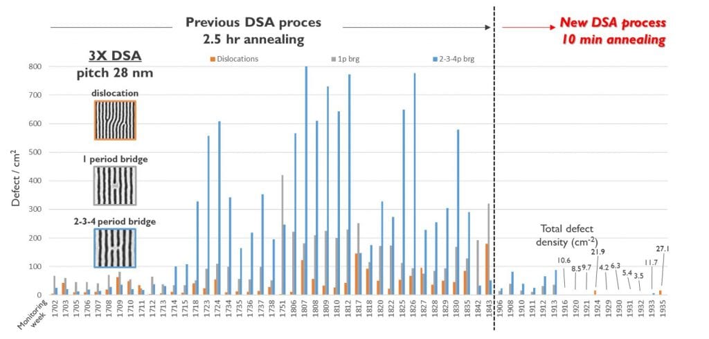
Defectivity: no longer a showstopper: Originally, the semiconductor industry was not so optimistic about DSA, because controlling the defectivity turned out to be very challenging. To be relevant for industrial manufacturing, the total defect density should be below 1cm-2 – which was very difficult to achieve at that time. Primary contributors to the total defectivity are dislocations and bridges, formed during the self-assembly process.
Today, however, imec is very confident to sufficiently control the defectivity. In recent years, imec has delved into the kinetics of defect annihilation and gained fundamental insights into how controlling dislocations and bridges. As a main result, the team was able to reduce the annealing time from an initial 2.5 hours to only 10 minutes, to obtain an ordered state with a stable and sufficiently low defect count. If we would use a conventional electron microscope, it would take more than a year to find out the defect. With these insights, imec can now provide the industry with a manual, containing the main knobs that allow to control the defectivity of the DSA process (Figure 1).

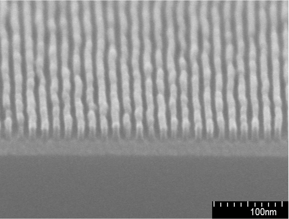
Towards a second generation of BCPs: Such stable and low defect DSA process was achieved by using 3x pattern density multiplication. A final pattern pitch of 28nm could be successfully patterned with DSA of BCPs on an 84nm pitch pre-pattern that was obtained with 193nm immersion lithography. The 3x pattern densification was enabled by using PS-b-PMMA (or polystyrene-block-poly methyl methacrylate) as a BCP.
As imec is moving towards sub-20nm pitches, the length of the BCP chain should be reduced as well in order to achieve smaller pitches. PS-b-PMMA polymers smaller than pitch 21nm will however not form a clear structure anymore, leaving the BCP in a mixed disordered state. To solve this issue, imec is now moving to a second generation of BCPs, i.e. high-χ BCPs – in close collaboration with material suppliers and universities. The learnings obtained so far with PS-b-PMMA have been transferred to this new generation of BCPs, leading to a good self-assembly process (Figure 2).

Currently, a few remaining issues are being investigated. First, the pattern transfer into the underlying materials is more challenging than expected in such tiny regime. And second, new metrology needs to be developed to be able to assess the defectivity of self-assembled structures that now have extremely small dimensions.
From university to imec, and to industry: About ten years ago, imec started exploring the idea of using DSA as an alternative patterning approach. At that time, DSA was mainly an academic field of research. Based on the progress made in recent years, DSA has now attracted large industrial interest. This evolution has been accompanied by a large commitment from universities, material and equipment suppliers, and from metrologists, to carefully control and inspect the materials and processes altogether. This ecosystem was the key to success, and it will be the same for the development of next generations of DSA processes.
ASD: depositing material only where needed
With area-selective deposition, a material is deposited according to a predefined pattern, while deposition on the rest of the surface does not occur. This selective deposition can be achieved by deposition techniques that rely on selective surface reactions, such as atomic layer deposition (ALD) and chemical vapor deposition (CVD).
A few years ago, also this bottom-up technique aroused the interest of the semiconductor industry as a complementary approach to traditional top-down patterning. Just like DSA, ASD comes with its own set of advantages. Compared to traditional lithography, it may enable a broader range of applications, such as patterning features in complex 3D structures. Another great opportunity for ASD is that it can in principle place structures only where needed, with atomic precision in both horizontal and vertical directions. This way, for some applications, it may become a more sustainable and cost-effective approach, requiring fewer chemical products and less energy compared to top-down patterning.
Until now, industrial use of ASD has been limited to the selective epitaxial growth of semiconductors and to growing nm-thin metal layers in interconnect structures, mainly because ASD has been studied only for a limited number of processes and materials. To expand the applicability of the technique, a fundamental understanding of the surface chemistry, of the surface dependence of the ALD and CVD processes and of the role of the precursors in these processes is essential. In addition, the ability to control or mitigate defects in the non-growth area is prerequisite. Since 2016, worldwide progress in this field is being discussed annually during the ASD Workshop. The increasing number of scientific contributions at this workshop reflects the growing interest of academia and industry into this fascinating field of research.
A growing insight into surface chemistry and modification: Imec has successfully explored several material systems that promise to enable the selective deposition of materials such as TiN or Ru, which are highly relevant for chip manufacturing. It was demonstrated, for example, that OH– terminated dielectrics like SiO2 can act as a growth surface for growing Ru. The same dielectric material, when terminated with CH3 groups, acts as the non-growth surface (or mask). The study confirms that both ALD precursors and reagents can further affect the selectivity, but the most straightforward way to extend the selectivity window is by surface passivation, via organic thin-film coating and/or plasma modification.
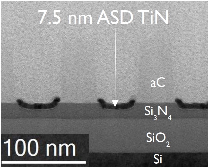
A second relevant material system involves amorphous carbon (aC) in combination with Si3N4 for the selective deposition of Ru, TiO2 or TiN. aC can act as the non-growth template, provided that the native oxide that exists on aC can be removed – for example by using H2 or halogenation plasmas. After the plasma treatment, Si3N4 remains reactive towards TiN ALD. Area-selective deposition of TiN has already been demonstrated on structures consisting of aC lines in combination with Si3N4 spaces (Figure 3). In addition, we investigate the fundamental mechanisms of ASD in nanoscale patterns, which can be different compared to regular thin-film deposition. This insight is crucial for the development of effective defect mitigation strategies for ASD.

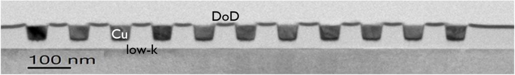
A wide range of potential applications: A deeper insight into the surface chemistry and growth mechanism during ASD will guide the design of novel ASD processes enabling a wider range of applications. Potential applications include for example the creation of fully self-aligned vias. Vias are metal structures that electrically interconnect the different metal layers in the chip’s back-end-of-line. Traditionally, via formation starts with the patterning of a via opening and etching it into an underlying layer. The via is then filled with metal (e.g. ruthenium (Ru)) and overfilled – meaning that the metal deposition continues until a complete layer of metal is formed over the underlaying layer. An etch step and a chemical mechanical polishing step complete the via formation (Figure 4). In this way, if the vias are oversized or misaligned there is a risk of shorts or reliability concerns. With ASD of dielectric on dielectric, on the contrary, thanks to the topography created, the specifications for alignment and oversizing of the vias can be relaxed.

Other potential applications are tone inversion processes, which, in general, allow to obtain inverse material patterns. As such, they can be used to turn holes into pillars, or spaces into lines. ASD is a promising technology for such applications. A pre-patterned, sacrificial layer is used as a template and the inverse material pattern is obtained through a bottom-up fill, by using area-selective deposition. Tone inversion with ASD can provide a solution when traditional lithographic patterning of the material is difficult, e.g. for hard mask materials such as TiN or Ru. Moreover, since no overfill and CMP steps are required, this solution requires less process steps than the traditional approach. ASD for tone inversion is also scalable towards smaller feature sizes. Imec is investigating the tone inversion application of ASD for line/space patterning and for self-aligned block patterning.
ASD is also a candidate for the bottom-up fill of extremely narrow trenches or holes such as the interconnect via, or even high-aspect ratio structures such as the Supervia, or for the vertical placement of features in complex 3D structures such as in the complementary field-effect transistor (or CFET). Potential applications are not limited to those listed here.
A disruptive approach: resist-free lithography: More disruptively, imec is exploring the potential of ASD as an alternative, resist-free approach to lithography, in support of the high-NA (0.55 numerical aperture (NA)) EUV lithography process. High-NA lithography is expected to become the next-generation EUV lithography process, promising to advance semiconductor scaling towards the sub-3nm technology node. EUV lithography with high numerical aperture optics typically requires very thin layers of photoresists, which are difficult to achieve uniformly. Moreover, current photoresist materials have very complex chemical compositions. When exposed to EUV light, the sidewalls between exposed and unexposed areas may show high roughness, which causes fluctuations in the effective feature size.
In parallel with searching for an optimal photoresist material for high-NA EUV lithography, imec is investigating the feasibility of creating a lithography patterning mask without using a photoresist material (Figure 5). The idea is to use surface modifications induced by EUV exposure to achieve a selective deposition of a hard mask material. There are several routes envisaged to this purpose. As an example, one of the ideas which was recently submitted as a patent idea (M. Krishtab, S. Armini) is to first provide a carbon-based material (such as aC or spin-on-carbon (SOC)) over the layer to be patterned. The top surface of this carbon-based layer is functionalized with halogen-containing groups (e.g. by using iodine or fluorine plasmas) to form ALD-blocking bonds. This surface is then exposed to EUV light, through a classical mask. In the exposed areas, secondary electrons will be released, breaking the bonds of the halogen-containing groups. A sensitizer layer is added to enhance the generation of secondary electrons within the surface. As a result, two different areas are formed: (1) an area that is selective towards ALD, and (2) an area that acts as a non-growth template. The target material (a metal, metal oxide or metal nitride) can now be selectively grown onto the first area by using ALD.

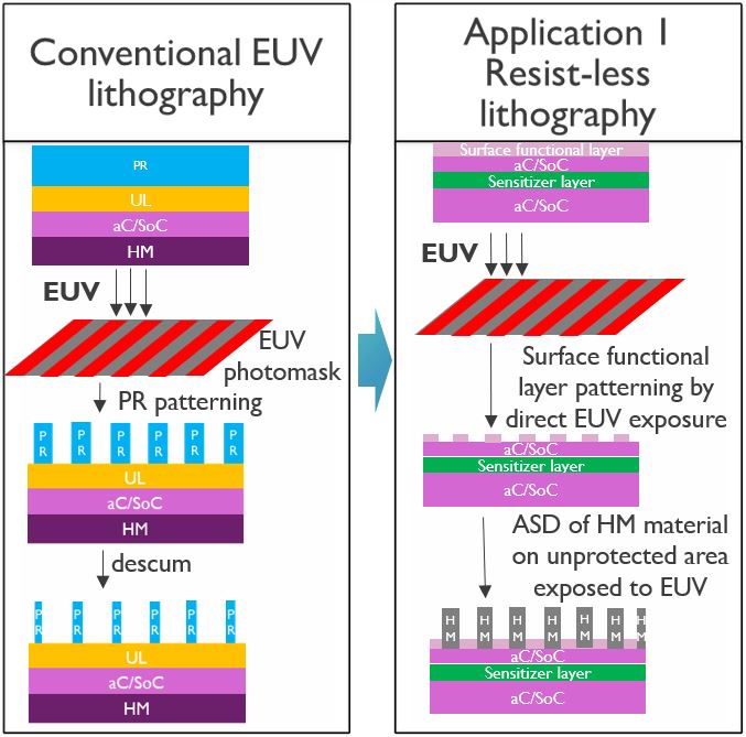
Just like traditional EUV lithography, resist-free lithography makes use of EUV photon emission. But in this case, only the top surface needs to be exposed to the light source, allowing to reduce the EUV dose needed for the exposure.
Today, the main goal of ASD-enabled EUV lithography is to build up fundamental understanding of the surface modification mechanisms, in combination with the area-selective deposition of relevant materials. In addition, a fundamental part of the work is to investigate the interaction of EUV light with the modified and unmodified material surfaces. This study is largely supported by modelling work, and by the tools that will soon become available within the Attolab. Attolab is a joint initiative of imec and KMLabs, recently set up to enable the study of EUV photon absorption and subsequent processes at unprecedented timescales, from attoseconds to picoseconds.
Summary
Both DSA and ASD have been presented as promising bottom-up patterning approaches that may be capable of complementing the traditional top-down patterning schemes. DSA is a champion technique when it comes to patterning dense, regular structures. Compared to conventional patterning, this technique promises a lower cost-of-ownership and a low edge placement error. Imec’s ability to control the defectivity has been an important step towards industrial uptake. ASD, on the other hand, is a novel approach allowing to place structures only where needed, with great precision. Provided that the surface chemistry, surface passivation and deposition mechanisms can be sufficiently understood, and defectivity can be controlled, the technology promises a broad range of applications for chip manufacturing – from tone inversion to resist-free lithography.
About the authors
Hyo Seon Suh is currently leading DSA activities at imec in collaboration with various industry and academia partners. Annelies Delabie is a principal member of the technical staff at imec and professor at the KU Leuven chemistry department. Silvia Armini is a principal member of the technical staff at imec.