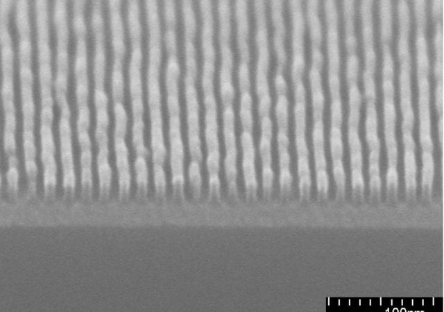
Rinse materials offer benefits of pattern collapse mitigation and defect improvement and, therefore, superior process margins for yield improvement. Defectivity is also significantly improved with an EUV rinse.
Building Patterns From The Bottom: A Complementary Approach to Lithography
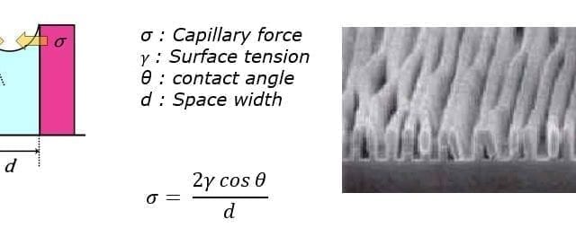
With shrinking dimensions, the classical lithography-based top-down patterning processes are becoming extremely complex and expensive. Therefore, researchers worldwide are investigating alternative processes allowing to build patterns from the bottom. Two promising approaches are directed self-assembly (DSA) and area-selective deposition (ASD).
Flagello to receive Zernike Award at SPIE Advanced Lithography
Donis Flagello, president, CEO, and COO of Nikon Research Corporation of America (NRCA), will be presented with the 2017 Frits Zernike Award for Microlithography on Monday 27 February during SPIE Advanced Lithography in San Jose, California. The award, presented annually…
Patterning with Films and Chemicals
Somewhere around 40nm is the limit on the smallest half-pitch feature that can be formed with a single-exposure of 193-nm wavelength laser light using water immersion (193i) lithography. While multiple-patterning (MP) is needed to achieve tighter half-pitches, smaller features at…
Trefonas Earns 2016 Perkin Medal
The Society of Chemical Industry (SCI), America Group, announced on May 5, 2016 that Peter Trefonas, Ph.D., corporate fellow in Electronic Materials at Dow Chemical Co (NYSE:DOW), has won the 2016 SCI Perkin Medal. This honor recognizes Trefonas’ contributions in…
Litho becomes Patterning
Once upon a time, lithographic (litho) processes were all that IC fabs needed to transfer the design-intent into silicon chips. Over the last 10-15 years, however, IC device structural features have continued to shrink below half the wavelength of the…
EUV Cost at 1000 Daily Exposures
On October 14, 2015, ASML Holding N.V. (ASML) published its 2015 third-quarter results: Q3 net sales of €1.55 billion with gross margin of 45.4% (in line with guidance), and guided Q4 2015 net sales at approximately €1.4 billion and a…