Wilbur Luo, vice president of product engineering for the Custom IC product group, replaces Michael Jackson, who served on the Si2 board since 2022.
Semiconductors
Fujifilm to Present Latest Advanced Lithography Research at SPIE Advanced Lithography + Patterning 2025 Conference
FUJIFILM Corporation today announced that two representatives from its Electronic Materials Research & Development Center, Keiyu Ou and Akihiro Hakamata, will present two papers on their latest research on advanced lithography technologies (specifically EUV Resist and EUV Developer as well as Nanoimprint Resist), at the SPIE Advanced Lithography + Patterning 2025 Conference (SPIE 2025).
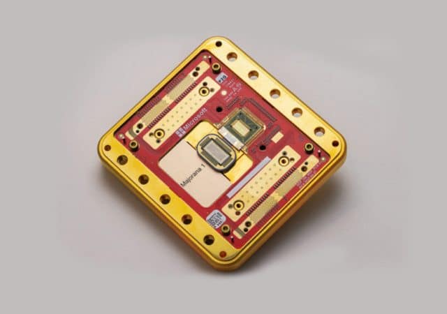
Microsoft Unveils Majorana 1, The World’s First Quantum Processor Powered by Topological Qubits
Built with a breakthrough class of materials called a topoconductor, Majorana 1 marks a transformative leap toward practical quantum computing.
PDF Solutions to Acquire secureWISE
PDF Solutions, Inc. today announced it has entered into a definitive agreement to acquire secureWISE, LLC, the most widely used secure, remote connectivity solution in the semiconductor manufacturing equipment industry, from Telit IOT Solutions Inc.
Texas CHIPS Act Awards Silicon Labs $23 Million to Expand R&D Advancements in Austin
Silicon Labs today announced the award of a $23 million grant from the Texas Semiconductor Innovation Fund (TSIF) established by the Texas CHIPS Act.
eBeam Initiative Member Companies to Take Center Stage at SPIE Advanced Lithography and Patterning Conference
Member participation includes eight keynotes and nearly 300 presentations; live member event to provide insight on lithography and photomask trends.

Global Semiconductor Manufacturing Industry Reports Solid Q4 2024 Results, SEMI Reports
The global semiconductor manufacturing industry closed 2024 with strong fourth quarter results and solid year-on-year (YoY) growth across most of the key industry segments.
Applied Materials Accelerates Chip Defect Review with Next-Gen eBeam System
Applied Materials, Inc. today introduced a new defect review system to help leading semiconductor manufacturers continue pushing the limits of chip scaling.
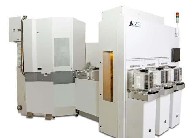
Lam Research Ushers in New Era of Semiconductor Metallization with ALTUS Halo for Molybdenum Atomic Layer Deposition
Lam Research Corp. today unveiled ALTUS Halo, the world’s first atomic layer deposition (ALD) tool that harnesses the capabilities of the metal molybdenum in the production of leading-edge semiconductors.
Lam Research Unveils Industry’s Most Advanced Conductor Etch Technology to Date
Lam Research Corp. today introduced Akara, a breakthrough innovation in plasma etch and the most advanced conductor etch tool available.