The proposed method produces wiring suitable for developing all-carbon devices, including flexible sensors and energy conversion and storage devices.
Semiconductors
SweGaN Launches Project for New Headquarters and Wafer Production Facility
The new facility will be built at the Innovative Materials Arena (IMA). IMA is cluster for innovative materials located in Linköping, Sweden, in Östergötland – a region renowned for its progressive materials industries.
2023 CMC Conference Announces Lineup of Speakers
Featuring talks on current trends, issues, and new technologies for the semiconductor materials supply chain.
imec’s Virtual Fab Underpins Strategies to Reduce the Carbon Footprint of Lithography and Etch Process Steps
This week, at the 2023 Advanced Lithography + Patterning Conference, imec presents a quantitative assessment of the environmental impact of patterning in advanced IC manufacturing.
EUV Tech and IBM Join the eBeam Initiative
The eBeam Initiative, a forum dedicated to the education and promotion of new semiconductor manufacturing approaches based on electron beam (eBeam) technologies, today announces the addition of two new company members to the organization.
MITRE Engenuity and Semiconductor Alliance Position Paper Outlines Guidance for National Semiconductor Technology Center Incubation
Ensuring the United States improves its global competitiveness in semiconductors requires strategic deployment of the $52.7 billion in funding authorized in the CHIPS + Science Act.
Samsung, Micron, and SK Hynix Account for Three-Fourths of Leading-Edge Wafer Capacity
At the end of 2022, Samsung, Micron, and SK Hynix accounted for 76% of leading-edge capacity, with the vast majority of it for advanced DRAM and 3D NAND production.
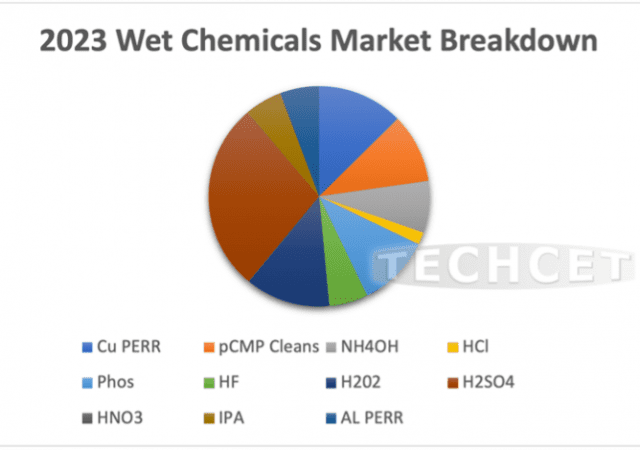
Semiconductor Wet Chemicals 1H2023 Trending Down
Although 200+ new layer chip offerings are expected in 2023.
Applied Materials’ Pattern-Shaping Technology Reduces the Cost, Complexity and Environmental Impact of Advanced Chip Manufacturing
Applied Materials, Inc. today unveiled a breakthrough in patterning technology that allows chipmakers to create high-performance transistors and interconnect wiring with fewer EUV lithography steps, thereby lowering the cost, complexity and environmental impact of advanced chipmaking.
Infinitesima Announces First Customer Shipment of Metron3D In-Line Probe Metrology System
Infinitesima have completed the first customer shipment of the Metron3D metrology system, a revolutionary sub-nanometer, high speed 3D imaging system that operates at in-line production throughputs.