Axiomise, the provider of cutting-edge formal verification consulting, training, services, and IP, today unveiled a comprehensive introductory certification-based formal verification training program to further the adoption of formal for hardware verification and validation.
Semiconductors
SEMI Provides U.S. Commerce Department with Analysis of Semiconductor Supply Chain Risks
SEMI today announced that it filed comments with the U.S. Department of Commerce in response to its request for public comments regarding risks in the semiconductor manufacturing and advanced packaging supply chain.
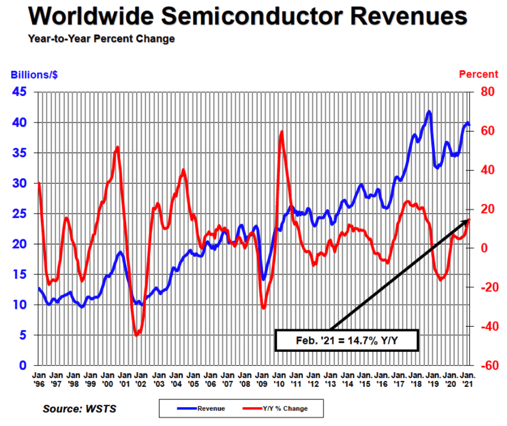
Global Semiconductor Sales Up 14.7% Year-to-Year in February
Worldwide sales decrease 1.0% month-to-month.

A New, Positive Approach Could Be the Key to Next-Generation, Transparent Electronics
A new study, out this week, could pave the way to revolutionary, transparent electronics.
ISS Europe to Explore Digitalization, Security and Environmental Sustainability
Leading executives, analysts, economists and technologists will gather 20-22 April, 2021, at the SEMI Industry Strategy Symposium Europe (ISS Europe), a virtual event, to highlight the technologies and the collaborations vital to meeting Europe’s most pressing strategic, social and economic challenges. Registration is open.
H.I.G. Capital Completes Acquisition of SMTC Corporation
H.I.G. Capital, a global alternative investment firm with over $43 billion of equity capital under management, announced that an affiliate has completed the acquisition of SMTC Corporation.
IIT Delhi Selects Samco Multi-Chamber CVD System for Developing Heterojunction with Intrinsic Thin-layer Solar Cell
Samco, a manufacturer of plasma processing equipment for the compound semiconductor industry, announced that the Indian Institute of Technology Delhi (IIT Delhi) has selected a Samco Multi-Chamber CVD system to develop a Heterojunction with Intrinsic Thin-layer (HIT) solar cell.
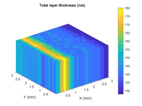
Multilayer Thickness Evaluation of Semiconductor and Display Structures by Picosecond Ultrasonics
The product line JAX designed by Neta uses unique properties of femtosecond pulses and photo-acoustic effects to inspect thin films stacks. This 100% non-destructive optical method can be used to test and control multilayers which are typical from applications in the semiconductor or in the display industries.
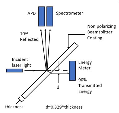
LiDAR Laser Circuit Optimization and Measurement
A method of measurement is described that provides the necessary feedback to correctly evaluate laser diode and driver performance and changes in spectral response with temperature simultaneously.
SEMI Applauds Initiatives to Bolster Semiconductor Manufacturing and Research in American Jobs Plan
SEMI today applauded the inclusion of initiatives to strengthen U.S. semiconductor manufacturing and research and calls for investment in the Biden Administration’s American Jobs Plan.