OBDUCAT AB (publ) subsidiary Obducat Technologies AB, a supplier of lithography solutions based on NIL (nanoimprint lithography), now launches the new tool platform Sindre Integra.
Semiconductors
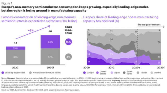
Europe’s Urgent Need to Invest in a Leading Semiconductor Ecosystem
Today’s chip shortage has put a spotlight on the degree to which the European economy depends on semiconductors. With limited local production capability and capacity, Europe risks its technological sovereignty and needs to correct course to maintain long-term competitiveness.
Acorn and UCLouvain Professor Collaborate on Groundbreaking Silicon-on-Insulator Research Project
Acorn Technologies today announced a research collaboration with Jean-Pierre Raskin, PhD, a full professor at the Université catholique de Louvain (UCLouvain), Belgium’s largest French-speaking university.
Mitsubishi Chemical Corporation Announces Expansion of Semiconductor Precision Cleaning Operations
Mitsubishi Chemical Corporation will invest over 10 million Euro for an expansion of its precision cleaning facility in Dresden, Germany.
RSBG Advanced Manufacturing Technologies GmbH Acquires Majority of Shares from Osiris International GmbH
RSBG Advanced Manufacturing Technologies GmbH (RSBG AMT), an investment company founded in 2019 and a wholly owned subsidiary of RSBG SE headquartered in Essen, Germany, holds 75.1% of Osiris International GmbH, headquartered in Singen, Germany, with retroactive effect from Jan. 1, 2021.
YES Announces Strategic Partnership with Osiris for Edge Film Removal Technology
YES (Yield Engineering Systems, Inc.), a manufacturer of process equipment for semiconductor advanced packaging, life sciences and “More-than-Moore” applications, today announced that it has signed an exclusive agreement with Osiris (Osiris International GmbH) to license its smartEBR technology for edge bead removal on panels.
Fraunhofer ENAS Successfully Manufactures Ultra-Thin and Highly Flexible Parylene-Based Printed Circuit Boards with Several Metallization Layers
Scientists at the Fraunhofer Institute for Electronic Nano Systems ENAS in Chemnitz successfully developed and manufactured flexible printed circuit boards with an overall thickness of less than 20 micrometers and several metallization layers based on the polymer Parylene. The institute presents the new generation of flexible PCB this fall at the COMPAMED and the SEMICON Europa 2021.
Gwangju Institute of Science and Technology Makes Breakthrough on New Electronic Material
New research reveals the easy tunability of a perovskite material, opening doors to its widespread use in next generation electronics.
Smart Textiles: High Performance, Breathable Fabric to Power Small Electronics
Scientists have created a new triboelectric fabric that generates electricity from the movement of the body while remaining flexible and breathable.
EV Group Brings High-Speed High-Precision Metrology to 3D Heterogeneous Integration
EV Group today unveiled the EVG 40 NT2 automated metrology system, which provides overlay and critical dimension (CD) measurements for wafer-to-wafer (W2W), die-to-wafer (D2W) and die-to-die (D2D) bonding as well as maskless lithography applications.