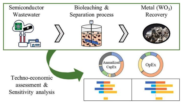
Semiconductor industry waste is typically seen as a costly disposal problem and an environmental hazard. But what if this waste could be transformed into a valuable resource?
Semiconductors
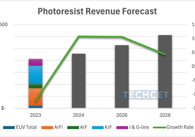
Lithography Materials Headed for Upwards Growth
PFAS elimination efforts expected to drive migration to photoresist alternatives.
Apple Is America’s Semiconductor Problem
If Apple wants to source its chips for pennies from foreign suppliers, it should have to pay a price to do so, such as a duty on imported iPhones using only foreign-sourced chips. Realizing the promise of the CHIPS Act depends on acknowledging and addressing Apple’s outsized influence over our domestic chip industry.
Entegris Enters Into Long-Term Supply Agreement with onsemi
Entegris, Inc., a supplier of advanced materials and process solutions for the semiconductor and other high-technology industries, announced it has entered into a long-term supply agreement with onsemi, a leading manufacturer of advanced energy-efficient power semiconductors.
ACM Research Strengthens its Fan-Out Panel Level Packaging Portfolio with Launch of Ultra ECP ap-p Tool
ACM Research, Inc., a supplier of wafer processing solutions for semiconductor and advanced wafer-level packaging applications, today announced its new Panel Electrochemical Plating (Ultra ECP ap-p) tool designed for fan-out panel-level packaging (FOPLP).
New Substrate Material for Flexible Electronics Could Help Combat E-Waste
Electronic waste is a rapidly growing problem, but this degradable material could allow the recycling of parts from many single-use and wearable devices.
New SEMI Foundation and Policy Equity Group Collaboration Earns Funding to Address Semiconductor Industry Child Care Gaps
Seeking to bolster the semiconductor industry workforce in the U.S. by addressing gaps in child care needs, the SEMI Foundation and Policy Equity Group today announced a collaboration to help companies comply with child care requirements under the U.S. CHIPS and Science Act.
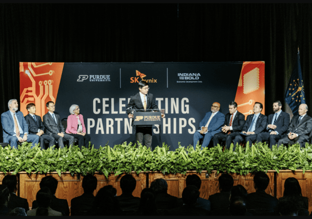
U.S. Department of Commerce Announces Funds to SK hynix’s AI Memory Chip Facility
The preliminary memorandum of terms between the South Korean semiconductor manufacturer and the U.S. Department of Commerce will support high-bandwidth-memory AI chip production and advanced packaging R&D.
Insight Global Launches Semiconductor Apprenticeship Program to Address Talent Shortages
Insight Global announced the launch of its new U.S. Department of Labor-approved Semiconductor Apprenticeship Acceleration Program (SAAP).

NEO Semiconductor Announces the Development of its 3D X-AI Chip
NEO Semiconductor, a developer of innovative technologies for 3D NAND flash memory and 3D DRAM, announced today the development of its 3D X-AI chip technology, targeted to replace the current DRAM chips inside high bandwidth memory (HBM) to solve data bus bottlenecks by enabling AI processing in 3D DRAM.