Abhijeet Joshi,Jalal Ashjaee and Bulent M. Basol, Active Layer Parametrics Inc. (ALP), Scotts Valley, CA
Development of next-generation semiconductor technologies is coming at enormous cost, ranging from hundreds of millions to several billion US dollars in process development for a new chip, spreading over long periods of time [1,2]. Only the few leading chip manufacturers can afford to explore advanced potential designs beyond FinFET. Metrology is a key factor for enabling accelerated development of such solutions by bringing down the overwhelming design cost. Besides the issues surrounding the architectures for next-generation nodes, new semiconductor materials are also required to be employed in advanced higher performance devices. These materials need to be fully investigated and accurately characterized in every aspect.
Active Layer Parametrics (ALP) recently developed and introduced a semiconductor electrical characterization technique called Differential Hall Effect Metrology (DHEM) [3]. DHEM provides depth profiles of critical electrical properties through semiconductor layers at nanometer-level depth resolution. DHEM is based on the Differential Hall Effect (DHE) method, which makes successive sheet resistance and mobility measurements on a layer using Hall effect and Van der Pauw techniques as the thickness of the layer is reduced through successive processing steps, typically involving chemical or electrochemical etching or oxidation. The data obtained as a function of thickness removed can then be used to determine the depth profiles of carrier concentration, resistivity and mobility. DHE has not been widely used in the semiconductor industry, because it is a slow laboratory technique requiring access to wet chemical processing facilities for etching and cleaning substrates multiple times before each electrical measurement. Also, the accuracy and depth resolution of DHE is very limited because of its manual nature. In contrast, the DHEM technique is a fully automated, fast, and high depth resolution (≤1nm) approach integrated into the ALProTM electrical depth profiling tools, making the technology affordable and practical to use for the first time for general purpose.
In a DHEM measurement, first a test-pattern such as a Van der Pauw cross, is prepared on the coupon sample to be characterized. The cross has a mesa structure isolating the top film to be characterized from its surroundings. It is also important that there is an insulating barrier electrically separating the top film from the substrate below, otherwise the electrical measurements would be compromised by substrate effects. The insulating barrier may be an oxide layer, a semi-insulating substrate or a p-n junction (i.e. the film to be characterized may be an n-type film formed over a p-type substrate, or vice versa). Four electrical contacts are formed at the ends of the four arms of the test-pattern and the nozzle of a small process chamber delivering chemical solutions, DI water or nitrogen gas is sealed against an area including a test region in the middle of the cross-shaped test-pattern. The size of the test region can typically be adjusted from 0.5mm x 0.5mm to 2mm x 2mm so that the data collected is representative of that area. Through chemical and/or electrochemical means the electrically active thickness of the layer at the test region is reduced in a stepwise manner and measurements of sheet resistance and mobility are carried out after each thickness reduction step using Hall effect and Van der Pauw techniques. Data collected may then be processed to yield depth profiles of resistivity, mobility, and carrier concentration. Figure 1 shows in sketch form the fundamentals of DHEM.
Material removal control
Depth resolution of the data obtained from DHEM depends on the smallest thickness of the semiconductor layer that can be controllably and repeatably removed from the test region. Electrochemical etching and oxidation are well suited for this purpose. However, there is a need for recipe development for each class of material to be characterized. Recipe development involves selection of the material removal process (etching or oxidation) as well as the proper chemistry. For materials that form stable oxides in dilute electrolytes, such as Si, oxidation approach is more attractive. For Ge with water soluble oxide, on the other hand, an electrochemical etching approach may be utilized. In any case the removal process needs to be calibrated so that the thickness of material removed can be monitored and controlled. For Si, using the anodization voltage as the variable, it is possible to control material removal as thin as 0.3nm steps. For Ge, using charge passed through the anodization circuit as the process monitor, one can control material removal to the tune of 0.5nm steps. Therefore, sub-nm depth resolution is possible to achieve in DHEM.
Application examples
DHEM can be used in all applications where knowledge of the behavior of electrical properties through a semiconductor layer or at film interfaces is valuable to semiconductor and device process engineers and those involved with device design and modelling. Comparison of SIMS depth profiles, which show variation of chemical composition through a layer, with the DHEM data is especially powerful for establishing relationships between chemical and electrical properties and for studying the correlation between process parameters and film quality. Some of the application areas of DHEM include dopant activation optimization (ion implantation, plasma doping, RTP/laser/flash annealing), ultra-shallow junction measurements, epi-layer optimization (sheet resistance, mobility, carrier concentration as a function of depth and process parameters) and composition/defectivity/stress/mobility correlations in layers such as novel p-well, n-well regions [4,5]. The following paragraphs will present examples to demonstrate the use of this technique for some of these applications.
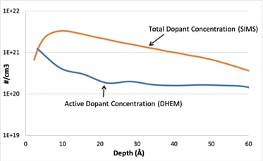
Determination of dopant activation through a semiconductor layer is very important for development and optimization of doping/annealing techniques. As transistor size is reduced, series resistance due to source/drain contacts needs to be lowered as well since it greatly limits device performance. In such an application, it is crucial to know the dopant activation within the top 5nm of the highly doped region. This requires a technique with capability to depth profile carrier concentration with sub-nm resolution. Figure 2 shows the SIMS and DHEM depth profiles taken from a P-doped epi-Si film. Phosphorus doping was achieved by ion implantation followed by a millisecond annealing step. As can be seen from this data, although the total P concentration as measured by SIMS is over 1021/cm3 within the top 2nm of the film, the carrier concentration represented by the active portion of the dopant is in 1020/cm3 range. Furthermore, activation is the highest within the top 1nm of the film, which is desirable for good ohmic contact formation.

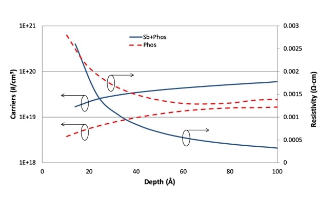
In another example, doping efficiency in the surface region of n-Ge was studied by DHEM.As it is widely known, Ge is a promising channel material for advanced transistor structures due to its high carrier mobility; but it is difficult to make low resistance contacts to Ge NMOS. This is in large part due to poor dopant activation in n-Ge caused by point defects. Figure 3 shows the results of a study on co-doping, which had been previously shown to reduce defect density in Ge. Samples were epi-Ge layers grown on Si substrates. The first sample was implanted with only P (dose 6×10¹⁴/cm2, 90 keV), and the second sample was implanted first with Sb (dose 6×10¹⁴/cm2, 65 keV) followed by P (dose 6×10¹⁴/cm2, 90 keV). Both samples were then annealed at 500°C for 10 s in N2 to activate the dopants. As can be seen from Figure 3, the near-surface active dopant concentration in P-doped sample is ~5×10¹⁸/ cm3 despite the fact that SIMS measurement showed a P concentration of ~1020/cm3. With co-doping with Sb and P the near-surface active dopant concentration increases to ~2×10¹⁹/cm3. It is also noted that the resistivity of the co-doped material is appreciably reduced in the top 10nm thick section. In the same study it was also determined that although dopant activation and resistivity were reduced near the surface of co-doped sample, mobility values were reduced compared to the P-doped material. This reduction in near-surface mobility could be an effect of the residual damage left in the top surface of the co-doped sample and could possibly be optimized through optimization of the annealing step.

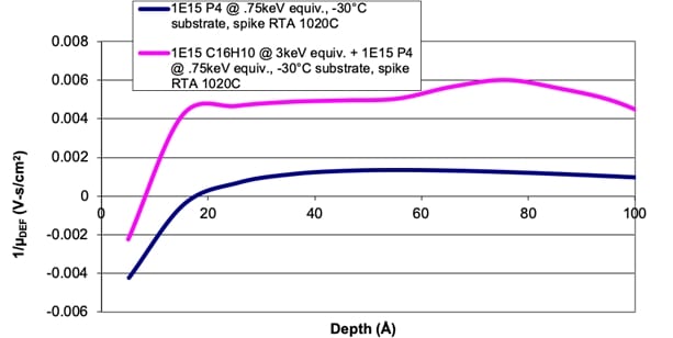
DHEM can also be used to study mechanisms influencing carrier mobility in semiconductor layers. Determination of defect scattering contribution to mobility reduction from implant damage, for example, may be investigated by comparing DHEM data obtained for a material like Si to ASTM model expectations. As is commonly known, Matthiessen’s rule given in equation (1) below represents the approximate relationship between the measured mobility, µ, of a highly doped thin film material, and the mobility, µ0, of fully-relaxed, moderately doped single crystal. The values given by ASTM model can be considered to represent µ0, and they may include the effects of lattice scattering and scattering due to impurities introduced in the lattice in amounts within the solid solubility limit. The term µDEF, on the other hand, is the mobility dominated by defect scattering and possibly strain in a layer doped heavily using methods such as ion implantation followed by annealing. Comparing the mobility depth profiles obtained from DHEM to ASTM model mobility values can give valuable insight into how such scattering mechanisms may vary with doping process conditions.
(1/µ) = (1/µ0) + (1/µDEF) (1)
Figure 4 shows the (1/µDEF) values derived from DHEM measurements and equation (1) for the top 10nm of two Si wafers. One of these wafers had a C pre-implant (C16H10) and both were implanted with P as noted in the inset of Figure 4. Annealing step was a spike RTA at 1020 ºC. As can be seen from this data the sample with C pre-implant has a (1/µDEF) value that is ~ 5x greater indicating a substantial amount of mobility degradation due to the uncured defectivity left behind by the pre-implant process. It is also observed that degradation gets worse beyond 2nm from the surface. Negative values at the surface may signify mobility enhancement due to strain effects.

Conclusion
It is practical to acquire electrical property depth profile data from semiconductor films using Differential Hall Effect Metrology (DHEM) approach. The technique can yield sub-nm depth resolution for Si and Ge. For III-V compounds depth resolution is ~1 nm. Mobility and carrier concentration depth profiles are useful in understanding dopant activation and defectivity in the film, especially in the near-surface region, and correlation of these with process conditions. Through recipe development, it may be possible to carry out DHEM measurements not only through semiconductor films but also through insulator/semiconductor and metal/semiconductor stacks to elucidate electrical properties of the semiconductor layer under the top insulator or metal film close to the interface between the two layers. DHEM can be a valuable tool for fab manufacturers, process control engineers and developers, to be used along with more commonly employed characterization methods such as SIMS, 4-point probe, Spreading Resistance Profiling (SRP) and Scanning Spreading Resistance Microscopy (SSRM).
References
1. Joel Hruska, “As Chip Design Costs Skyrocket, 3nm Process Node Is in Jeopardy,” Extremetech, 22 June, 2018 <https://www.extremetech.com/computing/272096-3nm-process-node>.
2. Mark Lapedus, Big Trouble At 3nm, Semiconductor Engineering, 21 June, 2018, <https://semiengineering.com/big-trouble-at-3nm/>.
3. Active Layer Parametrics, Technology, <www.alpinc.net>.
4. J. Borland, S. Chaung, T. Tseng, A. Joshi, B. Basol, Y. Lee, T. Kuroi, T. Tabata, K. Huet, G.Goodman, N. Khapochkina and T. Buyuklimanli, “Boosting Ge-epi p-well mobility and crystal quality with Si and Sn implantation and melt annealing”, ECS Transactions, 86(7), 357-372 (2018).
5. J. Borland, S. Chaung, T. Tseng, Y. Lee, A. Joshi, B. Basol, T. Kuroi, G. Goodman, N. Khapochkina and T. Buyuklimanli, “Boosting Ge-epi n-well mobility with Sn implantation and p-well mobility with cluster-C implantation”, 22nd International Conference on Ion Implantation Technology (IIT), 16 September – 21 September, 2018, Wurzburg, Germany.
6. A.Joshi, S. Prussin, “Determining defect and strain effects on active layer mobility”, 20th International Conference on Ion Implantation Technology (IIT), 26 June – 4 July, 2014, Portland, Oregon.