DR. THOMAS UHRMANN, EV Group
With traditional 2D silicon scaling reaching its cost limits, the semiconductor industry is turning to 3D integration and heterogeneous integration—the manufacturing, assembly and packaging of multiple different components or dies with different feature sizes and materials onto a single device or package—in order to increase performance on new device generations. In this article, we will examine the importance of metrology at various key process steps to ensure successful production yields for heterogeneous integration devices.
As interconnect pitches in 3D packaging (3D-IC, 3D system on chip, etc.) become tighter with each new product generation, wafer and die bond alignment and overlay processes must also scale accordingly, with greater accuracy and more frequent measurements to identify process problems when they occur in order to provide corrective action or the possibility for rework, leading to higher production yields. On the other hand, fan-out wafer level packaging (FOWLP) in a chip-first/face-down configuration involves the use of temporary molded carrier substrates, which can cause challenges such as shifting die position and rotation due to mold warpage and shrinkage from the compression molding and debonding process. Measuring the die position with high accuracy is essential since interconnect densities and line/space (l/s) density are increasing. The introduction of maskless lithography provides an effective and versatile solution to tackle die shift through the use of adaptive patterning, which compensates for the misalign fingerprint of each die, system and wafer individually. However, this also drives the need for metrology that can deliver crucial information on die position wafer shape.
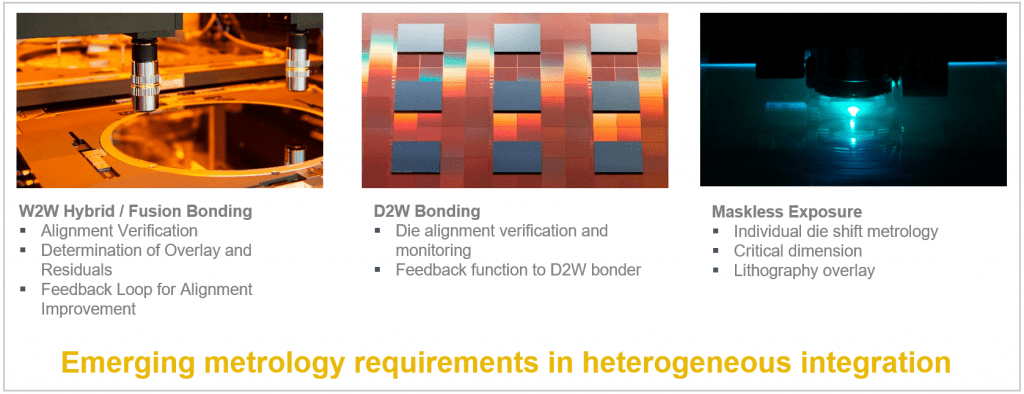
Collectively, these different heterogeneous integration process steps have a unique set of metrology requirements (FIGURE 1), which can be met by the EVG®40 NT series of automated metrology systems.

Integration pitch driving new metrology demands
System integration has been enabled mainly by different types of packages where dies with different functionality have been connected using standard interconnect technologies such as wire bonding and solder bumping. For these 3D systems in package (3D SiP) devices, interconnect pitches down to about 30µm are common. For silicon interposers and 3D stacked ICs such as stacked memory cubes, solder micro-bump interconnect pitches are scaling down to 10µm and below. 10µm pitch is setting a junction in interconnect technology. On the one hand, it is seen as the inflection point of hybrid bonding. At the same time, these extremely tight pitches enable functional partitioning of device functions onto different dies (chiplets) using die-to-wafer (D2W) hybrid bonding or wafer-to-wafer (W2W) hybrid bonding.
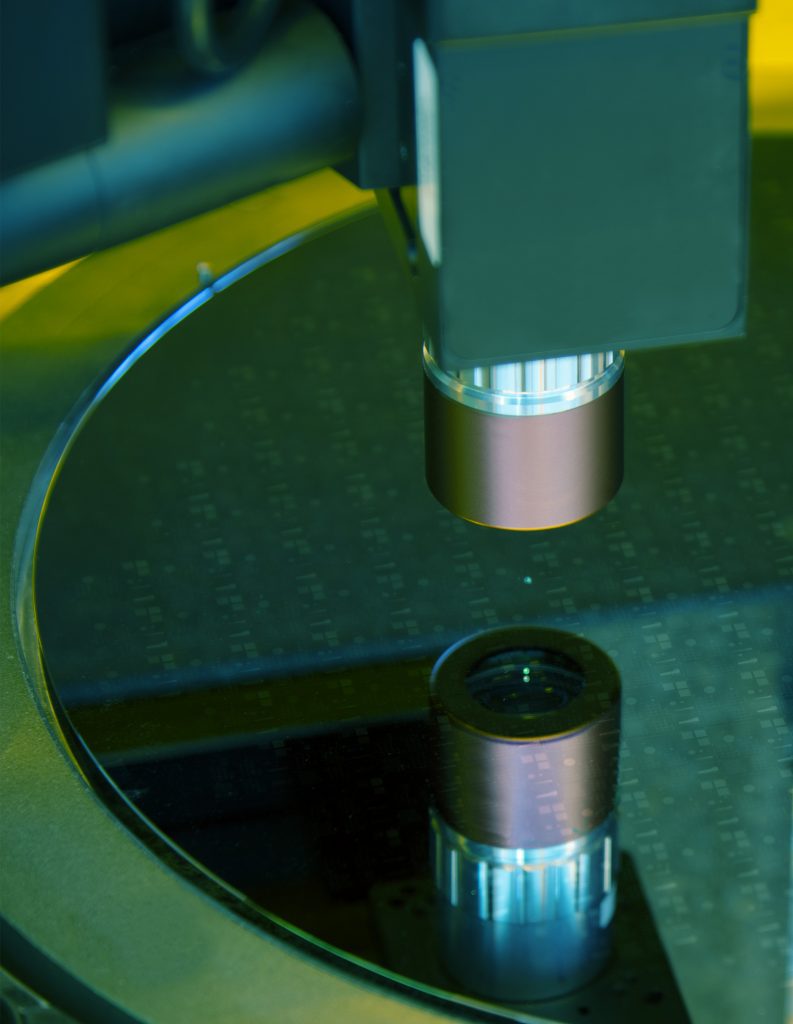
Metrology needs for W2W bonding
W2W bonding processes are enabling new device fabrication concepts, such as memory-on-logic devices through the transfer of memory layers like NAND, DRAM, SRAM or Flash from one wafer to another, as well as backside illuminated image sensors and other heterogeneous integration device applications. Improving overlay between wafers during W2W bonding enables the connection of different layers at earlier metal levels, which saves cost as well as increases device bandwidth and performance. For production of the first generation of image sensors about 10 years ago, W2W overlay in the range of 500nm to 1µm was sufficient. This has quickly scaled down with future device generations. Today, the multitude of applications and different integration scenarios give a wider requirement spectrum from 4µm interconnect pitches down to 500nm interconnect pitches in research. Consequently, W2W overlay requirements for leading-edge applications today range from 500nm down to 100nm overlay pitches.
Click here to read the full article in Semiconductor Digest magazine.