By AMANDINE PIZZAGALLI, Technology & Market Analyst, Equipment & Materials – Semiconductor Manufacturing, at Yole Développement (Yole).
The overall semiconductor equipment market is worth several billion dollars. By contrast, the lithography equipment market for the More-than-Moore (MtM) industry is a small niche representing millions of dollars. However, new emerging markets push MtM devices to new levels of complexity, resulting in big investments.
The semiconductor industry has traditionally been dominated by silicon substrates. Although silicon is by far the most dominant substrate with more than 80% of the market [1], alternative non-silicon-based substrates like GaAs, GaN, SiC and InP are gaining momentum within the MtM industry.
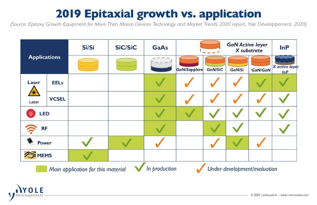
Indeed, as new applications emerge along with stringent requirements, those semiconductor substrate materials have started to be appealing for those applications where silicon can no longer meet the requirements. Some non-silicon-based substrates have already made serious inroads into the MtM market, such as GaN-on-sapphire technology for LED, GaN-on-silicon/SiC for power, SiC/SiC for power and RF as well as GaAs and InP for RF and photonics (Figure 1).

All these semiconductor substrate materials, silicon-based devices but also in the III-V compound semiconductor industry, require an epitaxy process step which is one of the first stages in manufacturing electronic and optical components consisting of depositing a mono-crystalline film on a mono-crystalline substrate. This process, which enables an improvement in the quality of the films, drives big opportunities in epitaxy growth equipment systems, such as MOCVD, MBE and CVD. The right epitaxy growth tool technology will strongly depend on the technical performance associated with the applications’ requirements, as well as the cost.
Indeed, requirements and epitaxy techniques for non-silicon-based devices – typically III-V compound semiconductor substrates – differ from those used in mainstream silicon-based semiconductor devices.
From a technical point of view, MOCVD represents the majority of the III-V compound semiconductor epitaxy industry, such as GaAs and GaN- based devices, while high-temperature CVD (HT CVD) is the mainstream deposition technology for silicon-based components, SiC devices and, generally speaking, for high voltage applications (Figure 2). They are in essence similar to the ones used in mainstream semiconductors except the process is established at a high temperature, above 1000°C. As such, they require redesign to reach optimum performance at the optimal cost of ownership.
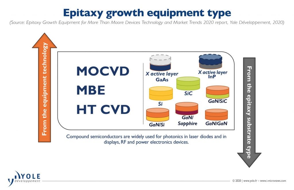
In terms of devices, MOCVD tools are very specific to the compound semiconductor industry, including LEDs, laser diodes and some power components based on SiC or GaN. They have been implemented in large volume manufacturing for LEDs, laser diodes and RF devices since the late nineties. Alternative technologies are already used in some applications or are emerging as potential competitive solutions to MOCVD, such as MBE. MBE, however, remains limited and dedicated to some R&D applications of GaAs or InP-based RF components and no breakthrough technology is expected to significantly alter the industry landscape in the mid-term (Figure 3).
In terms of the market, most of the equipment forecasts for More-than-Moore applications are calculated from a base scenario assuming much lower-scale adoption. However, the equipment market for both LEDs and microLEDs are very complex to analyze. Therefore, two scenarios, base and aggressive, have been considered for the market forecast as it is challenging to predict what is going to happen exactly.
For instance, investment in epitaxy growth equipment for traditional LED devices does not follow wafer demand trends but is impacted by the overcapacity from Chinese LED makers. LED epiwafer/chip supply is now mostly in the hands of Chinese players, at least for low- and mid-power LEDs. The state of the epitaxy growth equipment market is a direct consequence of the Chinese government’s strategy of aggressively subsidizing LED companies at the LED chip level. Either companies receive significant subsidies for acquisition of MOCVD reactors but pull the plug and stop investing in the next few years due to reaching overcapacity, or all the main LED manufacturers in China continue overinvesting in MOCVD reactors.
Additionally, in the case of microLEDs, their adoption is fueled by luxury TVs, AR and HUDs, automotive applications and smartwatches in both scenarios. Apple will adopt microLEDs in its higher-end 2021 smartwatch model and thus will generate an additional driver for investment in MOCVD reactors.
However, the only difference between the base and aggressive scenarios is the potential entrance of smartphones. In the aggressive scenario, the bulk of microLED volume is driven by smartphones where epi-ready wafers could climb to close to 6.5 million 6-inch wafers per year [1], a scale similar to the existing LED industry in terms of volume. Despite the risk that the additional applications taken into consideration in this scenario might not happen, smartphones could drive up demand for microLEDs resulting in a strong increase in demand for MOCVD reactors. If successful in its initial years, the market would be far from saturated in 2027 and growth could accelerate further beyond that point. But there still is a significant risk that this application does not materialize at all.
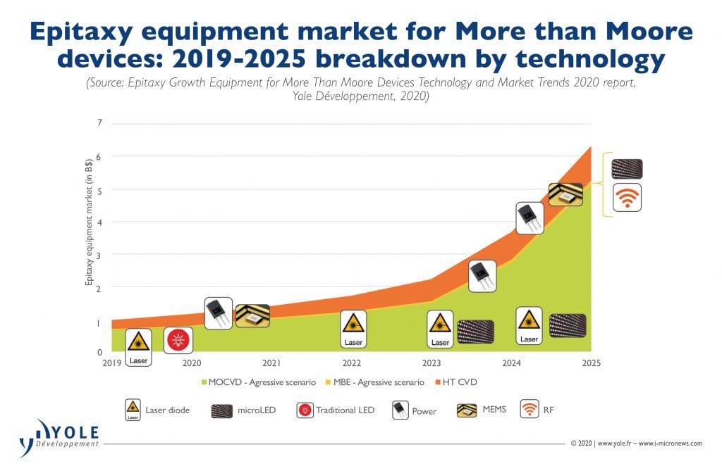
Meanwhile, laser diodes represent an additional fast-growing opportunity as the industry massively adopts edge-emitting lasers and VCSELs in the consumer space. On the contrary, MEMS and power devices make up a small niche proportion of the overall epitaxy growth equipment market as those markets are very well-established. As a consequence, the overall epitaxy equipment market, excluding MBE, is expected to increase from 522 tools in 2019 to more than 1213 tools by 2025 in the base scenario; more than 2000 in the aggressive scenario [1].
Corresponding revenue, almost $960M in 2019, will exceed almost $2.9B and $6.2B respectively in the base and aggressive scenarios by 2025 [1]. Revenue will be mainly generated by microLED and power SiC components as well as by laser diodes.
Currently, revenue is dominated by the mature LED device market, followed by power components. So far, RF devices do not represent significant volumes and remain a small fraction of the total epitaxy market revenue. Meanwhile, laser diodes and power applications are expected to experience rapid growth with a CAGR in the base and aggressive scenarios of 20% and 36% respectively in the timeframe 2019-2025 [1]. In point of fact, laser diodes represent another rapidly growing opportunity as the industry massively adopts edge-emitting lasers and VCSELs in the consumer space.
Generally speaking, from a technical point of view, MOCVD is leading the epitaxy growth equipment market, driven by laser diodes, LEDs and RF devices, followed by HT-CVD fueled by silicon-power- based devices and MEMS. An estimated seven MBE tools were shipped in 2018, corresponding to around $25M in revenue [1].
MOCVD seems to be the best available choice for GaAs-, GaN- and InP-based devices while high-temperature CVD appears to be the best option for SiC- and silicon-based devices (Figure 4). Indeed, due to the slow growth rate in MOCVD, high-temperature CVD will continue to dominate the power and MEMS markets. Nevertheless, MEMS and power will represent a small proportion of the overall epitaxy growth equipment market as these markets are very well-established.
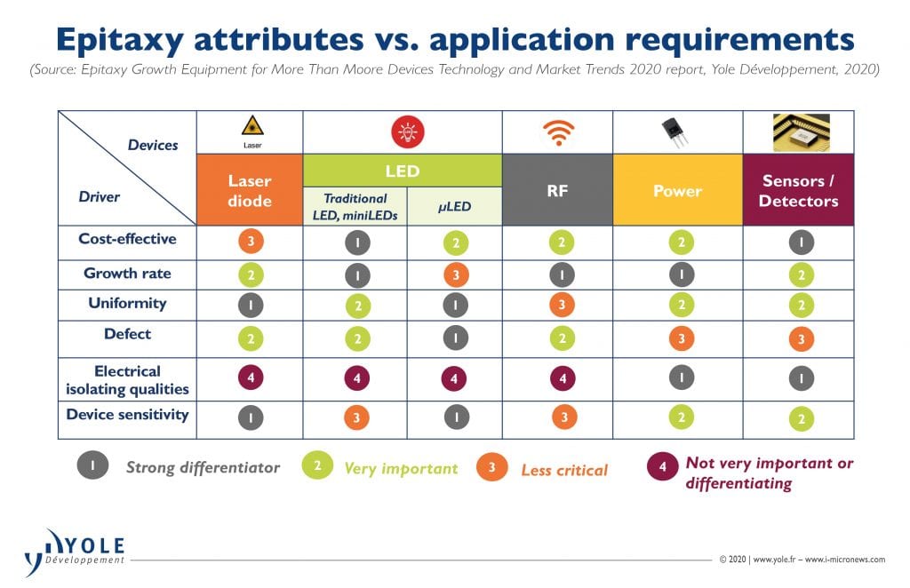
Currently, MBE is mostly applied to production of photonic ICs, detectors and PIN diodes. Although the technology imparts strong benefits for the Photonics InP-based applications and 5G operating in a range of 20Ghz, it is difficult to predict its exact impact in the short- and long-term.
In terms of market share, Aixtron, Veeco and AMEC represented almost 60% of the epitaxy growth equipment market in 2018 [1] as shown in Figure 5. Although the competitive landscape is occupied by a variety of equipment vendors, it can be segmented into two different groups due to the specifics of the business models and areas that companies are coming from. On one hand, top-tier semiconductor equipment suppliers like TEL and AMAT, coming from the front-end area, are offering CVD equipment optimized for the epitaxy process. They tend to support mainstream silicon applications while the other category employs specialist equipment vendors, like Aixtron, Nuflare, AMEC and LPE, that have developed their expertise in very specific MOCVD equipment lines where front-end suppliers do not have any products. Those typically serve the compound semiconductor-based market.
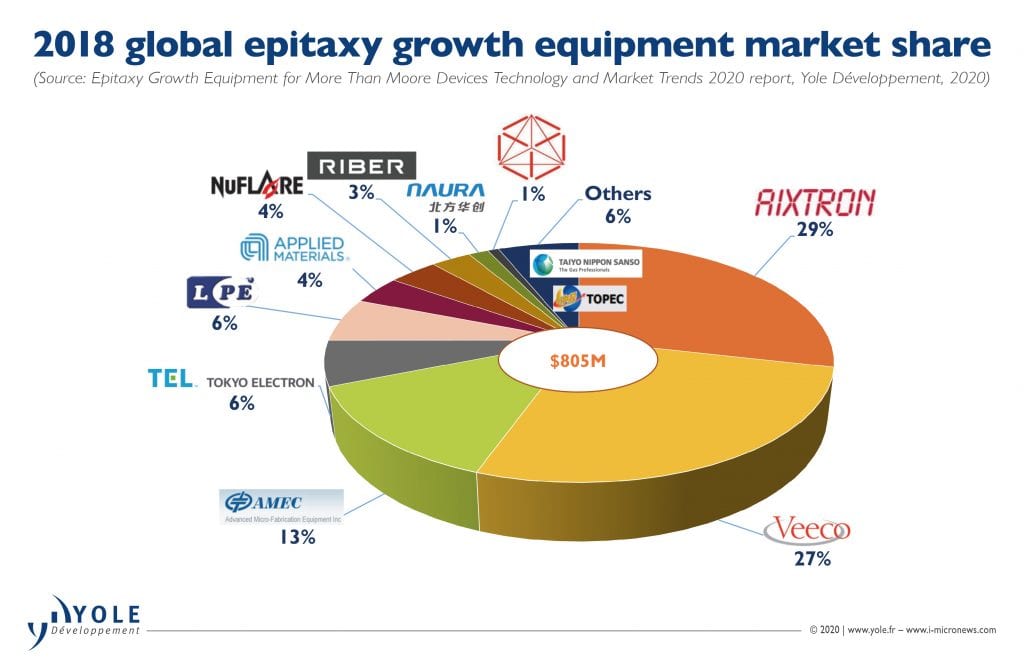
Aixtron is leading the GaAs market with a strong position in laser diodes as well as GaAs LED-based devices while AMEC is very well-positioned in the LED business. As a matter of fact, Aixtron seems to have developed a different strategy compared to its competitors, aiming at offering an equipment product portfolio for emerging GaAs applications like laser diodes and GaAs LED-based devices. Nevertheless, some emerging competitors, such as AMEC, have so far struggled to breach this monopoly. Between the complex relationships between China and the United States and the intellectual property dispute, Veeco has lost market share in China to AMEC. There is a risk that such disruption will continue due to trade barriers and additional taxes. These challenges might strongly impact Veeco’s share and reduce the competitiveness of Veeco in the Chinese market.
It would be difficult to compete with MOCVD giants like Aixtron, AMEC and Veeco, as these players have already made significant advances regarding MOCVD reactor manufacturing and design. To reshape the competitive landscape, new technical features should be offered by epitaxy equipment makers.
About the author
Amandine Pizzagalli is a Technology & Market Analyst, Equipment & Materials – Semiconductor Manufacturing, at Yole Développement (Yole). Amandine is part of the development of the Semiconductor & Software division of Yole with the production of reports and custom consulting projects.
References
1. Extracted from Epitaxy Growth Equipment for More Than Moore Devices Technology and Market Trends report, Yole Développement 2020.