TIMON EVENBLIJ, MANU PERUMKUNNIL KOMALAN, GOURI SANKAR KAR and ARNAUD FURNEMONT, imec, Leuven, Belgium
There was a time when the different steps needed to design and develop electronic systems were carried out in completely separated worlds. The engineers and scientists who populated the different worlds hardly talked to each other – there was no need for that – and each of them performed his own defined task in the best possible way.
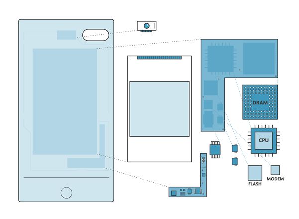
Think about an electronic system that we’re all familiar with: the mobile phone. It is mainly composed of a screen, a battery and computer chips: a central processing unit (CPU, the ‘brain’ of the phone), a dynamic random access memory (DRAM) memory block (the ‘working memory’ of the brain), a data storage unit, communication chips, power distribution chips and many other small components (FIGURE 1).

While mobile phone applications used to be simple (calling, texting, …) they quickly became more complex (video, web, apps). To handle these new applications, mobile phone makers continuously had to optimize their phone for better performance, while keeping power consumption under control. To do this, they had to optimize the chips that are inside the phone. In the world of material scientists and device engineers, they would approach this challenge at the technology level. They chose for example the right material and the most optimal dimensions to make the transistors which are the smallest building blocks inside the different sub-systems that form the CPU, DRAM, communication chip etc.
Once the job of the technology engineers was done, they passed the characteristics of the transistor (such as current, voltage and physical dimensions) to the world of the designers. Without needing to know any further details of the chosen technology, they used this information to start building complex circuits. They made the right design choices so that each circuit efficiently would do what it needed to do.
When the requirements for power and performance were met, the circuit output was transferred to the engineers that put everything together. By puzzling the circuits together in a real chip, they created cost-effective solutions to pass on to the world of the software engineers.
There, the engineers looked for the appropriate algorithms to run real applications, so that the consumer could make a call or browse the web. They evaluated the power consumption and performance of the complete system when running these applications, making sure the software used the hardware efficiently.
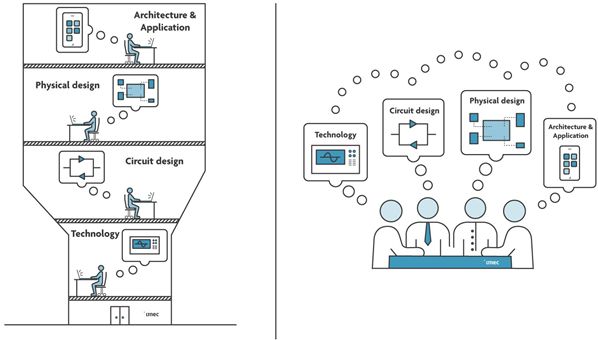
For a long time, this independent way of working was the most efficient way to master the complexity of designing systems. In those days, chips already contained millions of transistors, organized into larger components and circuits. Fortunately, each piece of the puzzle (i.e., technology, circuit design, physical design, application) could be optimized independently, bringing the desired benefits for the end user.
Today’s mobile phones have become faster than a mid-80s supercomputer, faster than the laptop that many of us are carrying around. Phones became increasingly complex and powerful. More and more sub-systems have been added, extending the functionality of the phone with video, voice recognition, 4/5G and Bluetooth connectivity, gaming etc. Billions of transistors now reside inside these handheld devices. Through the years, the awareness grew that optimizing these systems needed a different approach. Our engineers started to realize that every choice they made to solve a problem – be it at the technology, circuit design, physical design or application level – induced a new problem that affected the whole system. For example, the technologists could make transistors operate faster, as before, but soon realized that this was at the expense of power consumption. It became more and more clear that gains could only be made if they would remove the boundaries between their worlds, start to collaborate and co-optimize the system across the different ‘worlds’ (FIGURE 2).

In the semiconductor community, this evolution is referred to as design-technology co-optimization (DTCO), later complemented by system-technology co-optimization (STCO).
In an article published in the June/July issue of Semiconductor Digest, the authors further clarify the need for these approaches and explain how they work. Throughout the article, it also becomes clear how complex system design becomes when we leave the concept of separate worlds behind us. The authors introduce a unique simulation framework. This helps designers manage the complexity of performing cross-‘world’ optimizations – in order to enable the grand applications of the future.