PETE SINGER, Editor-in-Chief
Forty years ago, the semiconductor industry only used a handful of materials, such as silicon, silicon dioxide, silicon nitride and aluminum. Today, the industry employs 60+ different materials in increasingly complex device structures, such as 3D NAND, FinFETS, gate-all-around transistors. New materials now in play include chalcogenides, ferroelectrics (hafnium oxide and zirconium oxide), and specialty materials such as ruthenium and molybdenum.
The creation, modification, removal and analysis of these and other new materials is critical to the success of the semiconductor industry as it pushes to improve performance, power, area-cost and time-to-market (PPAC). Environmental concerns, such as greenhouse gas emissions, and supply chain issues are also of concern as new materials are introduced.
Materials development is very complex, on par with the complexity of the semiconductor manufacturing process itself. There are many experimental “knobs” to turn such as material composition and dopants, thickness, substrate, other neighboring layers, deposition method, precursors, anneal, etc. Each of these knobs causes changes in the materials such as phase, texture, crystal sides, defect density, thermodynamic stability, electrical and structural properties and degradation.
Ultimately, these materials must work flawlessly in a high volume manufacturing (HVM) environment. Here, real world considerations come into play, including purity, price, ease-of-handling, sustainability, byproducts, ease of disposal, and recycling/reuse options.
Speeding up innovation
One company that has taken a leadership role in the business of developing and supplying these materials is the Electronics business of Marck KGaA, Darmstadt, Germany which operates as EMD Electronics in the U.S. and Canada. The company supplies products for all essential production steps of wafer processing: patterning, deposition, planarization, etching, cleaning, doping and packaging. Its Silicon Valley innovation hub, Intermolecular, tests and develops advanced materials (FIGURE 1).

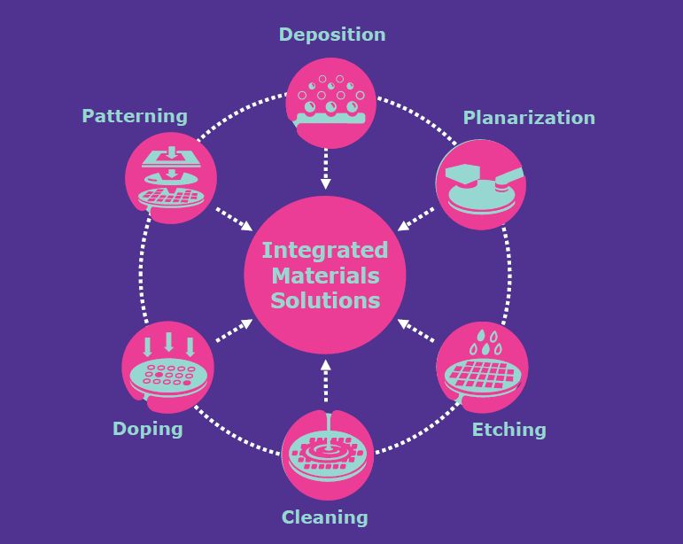
“We are the only company deeply experienced in every step of the semiconductor value chain covering all the front and back-end processes,” said Anand Nambiar, Global Head of Semiconductor Materials at EMD. “We have the industry’s broadest portfolio and capability to offer integrated materials solutions that produce the right materials combination to solve customers’ unique problems and help speed innovation with better yield.”
Read the full article in the December issue of Semiconductor Digest.