IBM likes to create a stir once in a while, and judging by the tech-press response in the last week or three they have achieved that goalwith their announcement of 2-nanometer CMOS technology, developed at their Albany research centre. A press briefing was hosted by Mukesh Khare (IBM VP of Hybrid Cloud Research) on the day before, and in it he claimed several technical firsts:
- The use of bulk Si wafers with bottom dielectric isolation under the nanosheet stack, reducing leakage and enabling 12-nnm gate lengths
- A 2nd-generation inner spacer dry process for precise gate control
- FEOL EUV patterning to allow nanosheet widths from 15 – 70 nm
- A novel multi-Vt scheme to enable multiple applications
This technology is expected to give a 45% performance boost or 75% power reduction, compared with a 7-nm process. Of course the question is, compared with what 7-nm process? In the Q&A Mukesh answered “What we are trying to do is align our work with 7-nm and 2-nm foundry technologies, and that’s what we are comparing it to, is 7-nm power and performance when compared to a 2-nm foundry power and performance, and that’s how we are comparing the two.”
IBM is currently getting ready to ship its POWER10 processors, fabbed in Samsung’s 7-nm node, so it is tempting to regard that as the 7-nm reference. There is no current 2-nm foundry technology, so that must be a guesstimate based on IBM simulations.
When it comes to transistor density, the press release states “this latest breakthrough will allow the 2 nm chip to fit up to 50 billion transistors on a chip the size of a fingernail.” Ian Cutress of AnandTech reached out to IBM and verified that their standard fingernail is 150 mm2, giving a transistor density of 333 MTr/mm2.The press briefing and release gave the impression that the 2-nm process was a single big breakthrough, but a more nuanced blog was published in parallel, noting that the advance was “the sum of several “Aha!” moments”, which actually makes a lot more sense. The 2-nm transistor was the cumulative integration of several developments over the last three or four years, including those listed in point form above.
The IBM GAA-FETS follow the trend in that they are three-stacks:

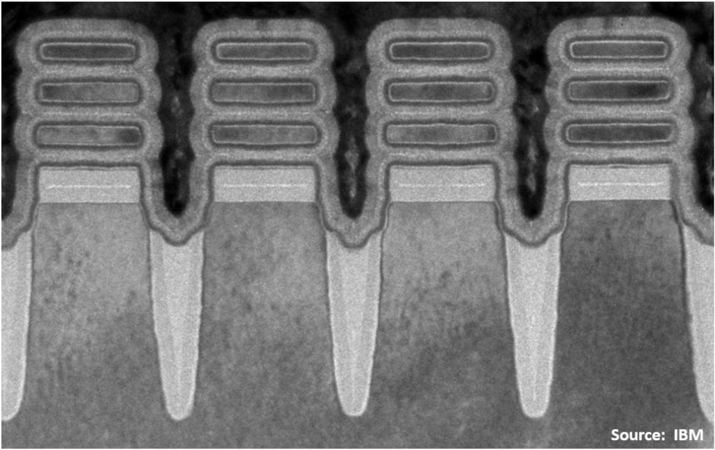
The bottom dielectric isolation (BDI) can be clearly seen between the substrate and the gate metallization under the lowest nanosheet. Based on the image density, I would guess it is silicon oxynitride – possibly nitride, but that has a higher dielectric constant.
For once we are actually given some dimensions:

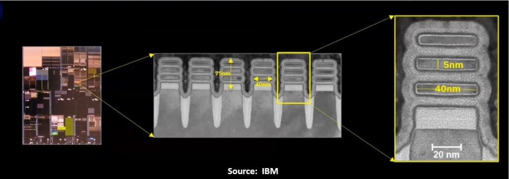
From the substrate up, the stack is 75 nm high, and in this sample the sheets are 40 nm wide and 5 nm thick, giving a gate width per stack of 270 nm (we are told that the nanosheets can vary from 15 – 70 nm).
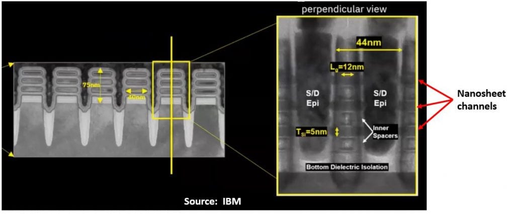
Taking a perpendicular section (i.e. channel direction), we were shown that gate pitch was 44 nm, and gate length 12 nm.

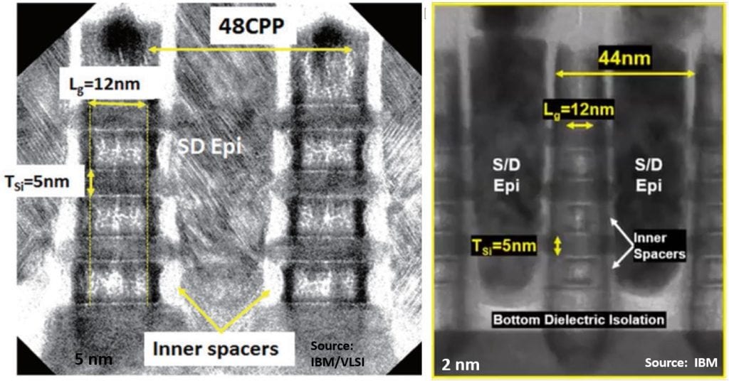
Checking back, these numbers are similar to the 5-nm process described at VLSI 2017 [1]. That had a dual CPP of 48/44 nm, shown at left below:

I guess that this just goes to show how logic node definitions are nothing to do with actual feature sizes any more, and more to do with marketing the next generation of performance and density improvements.
Bottom Dielectric Isolation
If we compare the 2-nm cross-sections with the 5-nm section, then we can see that the BDI is under both the nanosheets and the source/drain (S/D) epi. Without that isolation, the gate metal acts on the substrate, and the S/D epi is contacting the substrate, giving a “half-sheet” potential leakage path between source and drain.
One way around this is a punch-through stopper (PTS) doping in the substrate, but this is subject to process variations, and will likely be more sensitive as gate length scales down. Using BDI gets rid of the “half-sheet” problem and S/D junction doping variations in the substrate.
The introduction of BDI was detailed in an IEDM 2019 paper [2]; it appears that the first epitaxial SiGe layer for the nanosheet stack has a high Ge content compared with the upper sacrificial SiGe layers used to delineate the nanosheets. This seems to be etched out separately after stack definition and back-filled with what looks like oxynitride, though it looks as though it is formed in two steps.
The need for a selective etch for the two different Ge concentrations forced a reduction in the Ge% in the upper SiGe layers, and a consequent modification of the Si release etch to maintain selectivity and avoid etching the Si nanosheet channels.
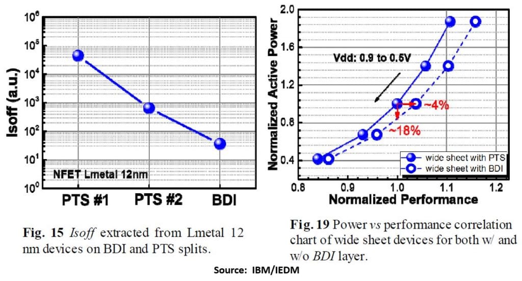
Below are two plots from the talk showing the reduction in leakage and improvement in performance compared with the PTS control, the latter due to a 4.4% reduction in Ceff for wide nanosheets (40 nm?) when BDI was used.

Inner Spacer Formation
Another IEDM 2019 paper discussed dry etching for forming the cavities in the SiGe layers for the inner spacers [3]. A 150:1 selectivity between SiGe25% and Si was achieved, controlling the NS inner spacer indentation shape with high precision.
The etch rate is strongly dependent on the Ge concentration:

Referring back to the SiGe etch for BDI formation, and looking at the above, it is tempting to speculate that the BDI SiGe is ~45% Ge, and the upper SiGe is in the 15 – 25% range. The authors state that faster etch B removes >50 nm SiGe 25% with no erosion of silicon. There seems to be enough differentiation in the etch rates that it is feasible to do the two separate etches. The inner spacer is needed to physically isolate the gate from the S/D junctions and reduce the S/D-gate parasitic capacitance. This schematic from TEL/imec [4] illustrates the steps for its formation:

After spacer etch the exposed part of the nanosheet is in effect the S/D extension, so controlling its thickness is critical, since Ron is inversely proportional and strongly dependent it [3]:

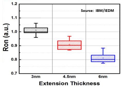
The final etched profile of the cavity is claimed to almost square, giving uniform extension thickness; the cavity depth (i.e. spacer thickness) can be accurately controlled to optimize overlap capacitance and Ron, and we can see that Cov drops significantly with a larger inner spacer at the cost of higher Ron [3].

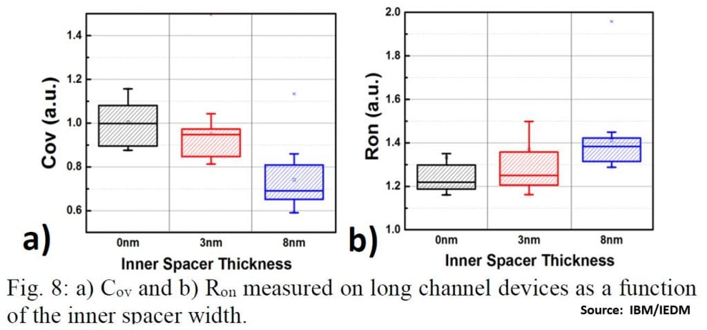
Examining the gate cross-section shown earlier, I guesstimate the spacer thickness in the 2-nm transistor to be ~5 nm, a good compromise looking at the above plots.
FEOL EUV Patterning
In the Q&A Mukesh said that they used the new ASML NXE:3400 EUV system that was installed last year, and the test chip used single patterning.
Multi-Vt Scheme
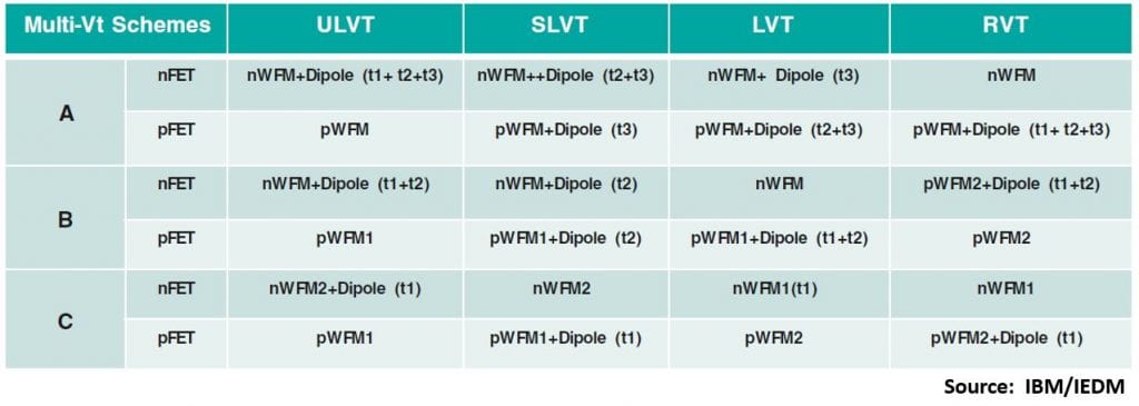
In a third IEDM 2019 paper [5], IBM discusses a multiple-Vt scheme which uses n- and p- work function metals (n- and p-WFM) plus dipole WFM tuning, and they claim the ability to create up to four pairs of Vts to enable applications from low power to high-performance computing.

We have seen something similar in finFET technology, using a combination of WFMs plus La doping to give extra Vt options (e.g. Samsung 10LPP in the Exynos 8910).
One of the limitations of replacement metal gate (RMG) high-k technology is the need to squeeze multiple metal layers into a shrinking gate length – here we are told that Lg is 12 nm, but when wrapping the gate metal around the nanosheets the gap between sheets could be less than that. We have a 5 nm sheet thickness, and I measure the distance between sheets as ~10 nm.
A conventional process sequence for defining NMOS and PMOS is to form the p-WFM all over the die, then mask the PMOS region and etch off the p-WFM in the NMOS areas. That’s fine for planar- or fin-FETs, but with nanosheets the masking resist gets between the sheets:

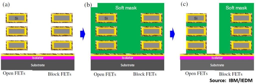
And in removing that there is a risk of etching back the mask at the edges of the PMOS zone.
IBM’s solution is to come up with a sacrificial material to fill the nanosheet gaps before resist deposition, which is removed selectively after PMOS definition without affecting the masked areas allowing p-WFM removal.

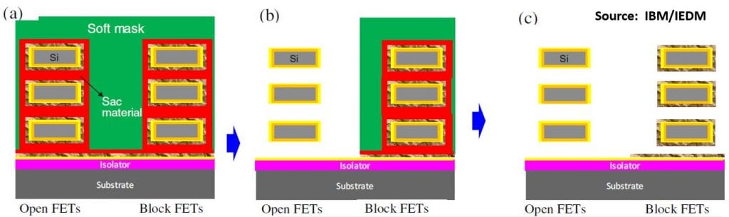
We are not given any clue as to what the sacrificial material could be.
However, all is not perfect in this new scheme, since removal of the n-WFM layer after resist removal in wide nanosheets (<100 nm) can erode the masking layers and etch back the edges of the p-WFM. To avoid this, the team came up with “metal gate boundary control” to protect the masked region, but no details are given.
Also in the Q&A Mukesh was asked if high-mobility SiGe channels were used – “No comment!”
Is it really 2-nm?
Over the weekend Scotten Jones of ICKnowledge published a blog on this topic on SemiWiki, and he came to the conclusion that a transistor density of 333 MTr/mm2 was more equivalent to a 3-nm process.
He plotted TSMC nodes versus transistor density and they matched a line with a 0.99 R2 value:

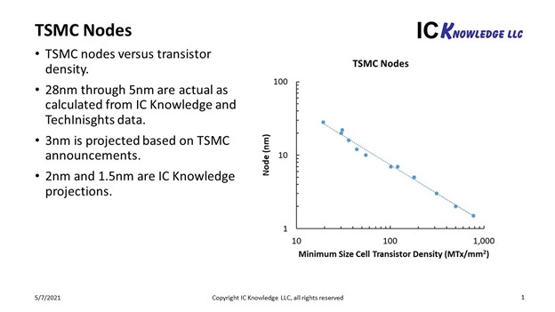
Fittting 333 MTr/mm2 on to this plot, Scotten came up with a “TSMC Equivalent Node” of 2.9 nm for the IBM announcement. This strikes me as a more objective way of assessing its place in the node spectrum, particularly as we have no information as to how IBM came with their number of 50B transistors in the first place.
IBM are estimating that this technology will go into production around the end of 2024; but they are not an IDM or foundry any more, so the first GAA foundry process is likely to be Samsung 3-nm, forecast for 2022 – 23. Since they are working with IBM on the 7-nm POWER10 parts, we will see if any of these features show up in their 3-nm product – or, given the new R&D collaboration with Intel, maybe Intel 5-nm.
References
- N. Loubet et al., “Stacked Nanosheet Gate-All-Around Transistor to Enable Scaling Beyond FinFET” VLSI 2017, paper T17.5, pp. T230 – T231
- J. Zhang et al., “Full Bottom Dielectric Isolation to Enable Stacked Nanosheet Transistor for Low Power and High Performance Applications”, IEDM 2019, paper 11.6, pp. 250 – 253
- N. Loubet et al., “A Novel Dry Selective Etch of SiGe for the Enablement of High Performance Logic Stacked Gate-All-Around NanoSheet Devices”, IEDM 2019, paper 11.4, pp. 242 – 245
- S. Kal et al., “Selective isotropic etching of Group IV semiconductors to enable gate all around device architectures”, SPCC 2018, https://www.linx-consulting.com/spcc-2018-technical-program/
- R. Bao et al., “Multiple-Vt Solutions in Nanosheet Technology for High Performance and Low Power Applications”, IEDM 2019, paper 11.2, pp. 234 – 237