IBM announced a breakthrough in semiconductor design and process with the development of the world’s first chip announced with 2 nm nanosheet technology. The new design is projected to achieve 45 percent higher performance and 75 percent lower energy use than today’s 7 nm chips.
IBM said this new frontier in chip technology will help accelerate advancements in AI, 5G and 6G, edge computing, autonomous systems, space exploration, and quantum computing, and extend the roadmap for IBM’s own technology offerings including IBM Power Systems and IBM Z platforms.
IBM announced the world’s first 7 nm test chip in 2015, followed by a 5 nm test chip in 2017 which employed the first instance of nanosheet technology for transistor formation. Mukesh Khare, IBM VP of Hybrid Cloud Research, said the 2 nm technology would likely not be in high volume production until 2024. IBM’s first 7 nm-based processor is debuting later this year in IBM POWER10.
In a press conference, Khare showed a cross-section of the 2nm chip (see Figure), noting six different transistors, each with three layers of nanosheet. Each sheet has a width of about a 14 nm and a height of about 5 nm. The transistor has a width of about 40 nm, which Khare said was the equivalent of two DNA strands. “That’s the level of atomic precision that is needed to put together this 2 nm nanosheet device structure,” he said. The pitch is about 44 nm, Khare said is what will likely will be used in the 2 nm foundry technology generation.

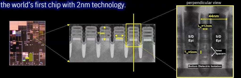
The new 2 nm chip includes several novel features: An industry-first bottom dielectric isolation (see Figure) to enable the 12 nm gate length, a 2nd generation inner spacer dry process for precise gate control; EUV patterning to produce variable nanosheet widths from 15 nm to 70 nm; and a novel multi-Vt scheme for both SoC and HPC applications.
Khare said the bottom dielectric isolation was important to reduce leakage current. The chip was built on a 300mm silicon bulk wafer. “The dielectric provides the reduction in leakage current that is needed to scale gate length to 12 nm,” he said.
EUV technology has been employed since the 7nm generation, but mostly for the middle-of-line and backend interconnects. Khare said it is the first time EUV has been used in the front-end for transistor formation. “Now, all the critical features will use EUV lithography. It essentially enables another knob for our designers, so they can have variable sheet width with anywhere between 15 to 70 nm,” he said.
The multi-Vt scheme enables threshold voltage control for the “entire range of application” from a handheld low power mobile application to a high-performance server application in a data center, Khare said.
The new chip does not employ stacked CMOS nanosheets, but that could be in the future. “In the announced 2 nm technology, we use nanosheet device architecture to deliver competitive density, power, performance to meet the technology requirements. Currently IBM Research Albany is also exploring technologies beyond 2 nm, jointly with our broad partnerships in the semiconductor ecosystem. Stacked CMOS is among several new device architectures we are exploring,” he said.
Replacing current chips with 2 nm-based processors could mean that hybrid cloud and other datacenter operators could even see drastic reductions in the energy costs and carbon footprint of their servers. Data centers account for 1 percent of global energy use, and changing all of their servers to 2 nm-based processors could potentially reduce that number significantly.
For consumers, these chips could potentially lead to cell phones that only need to be charged once every four days by quadrupling the average phone battery life within the same power envelope.
IBM’s partners include Intel and Samsung, with Samsung acting as the main manufacturing partner. “IBM has chosen not to invest in manufacturing and we work with our ecosystem partners to manufacture those for IBM,” Khare said. “That’s what we expect for two nanometer chips as well.”