By PROMOD CHOWDHURY, ROSE GUINO, KAIL SHIM, KEVIN LINDSEY, JIE BAI, GINA HOANG and RAMACHANDRAN TRICHUR, Henkel Corporation
As data demands and digitalization accelerate, new advanced packaging technologies including 2.5D and 3D integration are becoming the norm rather than the exception for many applications – particularly within the high-performance computing sector. To achieve the functional increases required for higher processing capabilities, efficiently integrating more I/O per die has given rise to the use of copper (Cu) pillars as a replacement for traditional solder bump flip-chip interconnects. This approach has been used for some time but Cu pillar and through-silicon via TSV designs, like other packaging techniques, are being challenged by complex assembly processes and resulting obstacles, including good alignment and reliable joint interconnections when bump pitch is less than 100 µm.

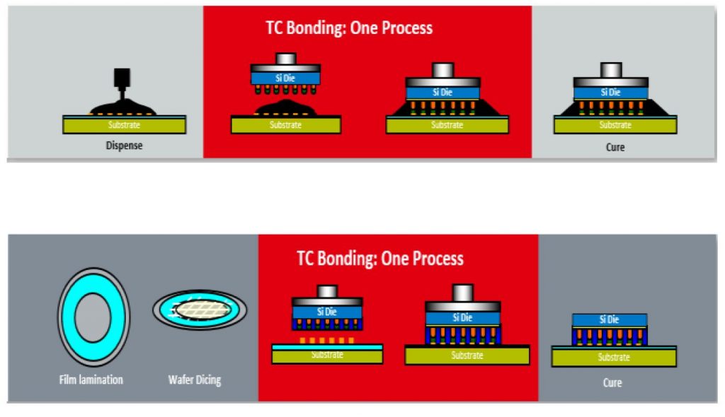
Using a thermocompression bonding (TCB) process (FIGURE 1) as opposed to a traditional C4 assembly process can help mitigate these concerns and the use of pre-applied underfills – whether paste or film – has shown excellent interconnect protective benefits. However, both non-conductive paste (NCP) and non-conductive film (NCF) underfills must be formulated for process compatibility, the assurance of good solder joint formation and void-free gap filling for maximum effectiveness. This paper will discuss recent analyses to understand optimization of NCP and NCF formulations, application considerations, and processing to ensure robust joint protection for next-generation Cu pillar chip designs.
Click here to read the full article in the October issue of Semiconductor Digest.