The IEEE 2022 Symposium on VLSI Technology and Circuits attracted 650 people to attend in person in Honolulu, and an equal number of virtual attendees.
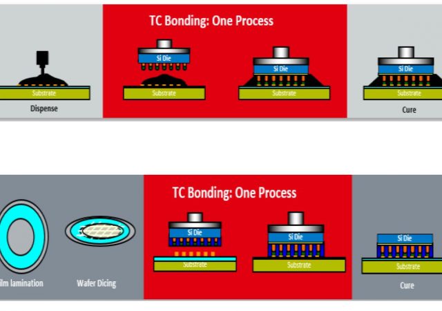
Maximizing Protection of Flip Chip Interconnects
NCP and NCF property and process optimization deliver high-reliability results.

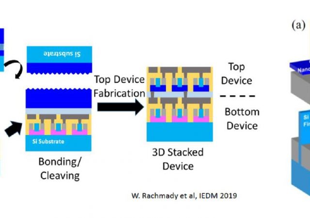
Intel 144-Tier Three-deck FG NAND with 161 Total Gates
A new 3D QLC NAND product has just arrived. TechInsights has quickly reviewed the Intel 1Tb QLC die removed from SSD 670p series which use 144L 3D NAND devices.
ASM’s Haukka ALD Award
Dr. Suvi Haukka, executive scientist at ASM International, located in Finland, was awarded the ALD Innovation prize at the ALD 2016 Ireland conference (Figure), as chosen by the conference chairs. Haukka has had a lifetime career in Atomic Layer Deposition…
Thermoplastically Deformable Electronic Circuits
Philips is testing a technology developed by imec and CMST (imec’s associated lab at Ghent University) to create low-cost 3D LED packages. As shown at last month’s International Microelectronics Assembly and Packaging Society (IMAPS 2015) meeting, these thermoplastically deformable electronic…
Micro-Buckled 3D Silicon Scaffolds
A new silicon microstructural solution announced this month is so powerful in creating 3D patterns from 2D surface machining that I just have to share. The figure shows 3D silicon microstructures formed by compressive buckling. The method can be used…
NanoParticle Self-Assembly at UofM
Theory and Practice synergize R&D Sharon C. Glotzer and Nicholas A. Kotov are both researchers at the University of Michigan who were just awarded a MRS Medal at the Materials Research Society (MRS) Fall Meeting in San Francisco for their…
Chasing IC Yield when Every Atom Counts
Increasing fab costs coming for inspection and metrology At SEMICON West this year in Thursday morning’s Yield Breakfast sponsored by Entegris, top executives from Qualcomm, GlobalFoundries, and Applied Materials discussed the challenges to achieving profitable fab yield for atomic-scale devices…
Moore’s Law is Dead – (Part 4) Why?
We forgot Moore merely meant that IC performance would always improve (Part 4 of 4) IC marketing must convince customers to design ICs into electronic products. In 1965, when Gordon Moore first told the world that IC component counts would…
Moore’s Law is Dead – (Part 3) Where?
…we reach the atomic limits of device scaling. At ~4nm pitch we run out of room “at the bottom,” after patterning costs explode at 45nm pitch. Lead bongo player of physics Richard Feynman famously said, “There’s plenty of room at…